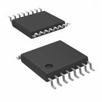
LM5115MTC/NOPB National Semiconductor, LM5115MTC/NOPB Datasheet - Page 5

LM5115MTC/NOPB
Manufacturer Part Number
LM5115MTC/NOPB
Description
IC CTRLR SSPR MULT OUTPT 16TSSOP
Manufacturer
National Semiconductor
Type
Step-Down (Buck)r
Datasheet
1.LM5115SDNOPB.pdf
(17 pages)
Specifications of LM5115MTC/NOPB
Internal Switch(s)
No
Synchronous Rectifier
Yes
Number Of Outputs
2
Voltage - Output
0.7 ~ 13.5 V
Current - Output
20A
Frequency - Switching
1MHz
Voltage - Input
4.5 ~ 75 V
Operating Temperature
-40°C ~ 125°C
Mounting Type
Surface Mount
Package / Case
16-TSSOP
Power - Output
300W
For Use With
LM5115EVAL - BOARD EVALUATION LM5115LM5115DC EVAL - BOARD EVALUATION LM5115DCLM5115AEVAL - BOARD EVALUATION LM5115A
Lead Free Status / RoHS Status
Lead free / RoHS Compliant
Other names
*LM5115MTC
*LM5115MTC/NOPB
LM5115MTC
*LM5115MTC/NOPB
LM5115MTC
Available stocks
Company
Part Number
Manufacturer
Quantity
Price
Part Number:
LM5115MTC/NOPB
Manufacturer:
NS/国半
Quantity:
20 000
VBIAS SUPPLY
VCC LOW DROPOUT BIAS REGULATOR
SOFT-START
ERROR AMPLIFIER and FEEDBACK REFERENCE
CURRENT SENSE AMPLIFIER
SYMBOL
Absolute Maximum Ratings
If Military/Aerospace specified devices are required,
please contact the National Semiconductor Sales Office/
Distributors for availability and specifications.
Electrical Characteristics
LO or HO.
VccReg
Supply Voltage, VBIAS
Supply Voltage, VCC
Supply voltage bypass, CVBIAS
Reference bypass capacitor, CVCC
HB-HS bootstrap capacitor
SYNC Current Range (VCC = 4.5V)
RAMP Saw Tooth Amplitude
VOUT regulation voltage (VBIAS min = 3V + VOUT)
VREF
GBW
Ibias
Vio
VBIAS to GND
VCC to GND
HS to GND
VOUT, CS to GND
All other inputs to GND
Storage Temperature Range
Junction Temperature
VBIAS Supply Current
VCC Regulation
VCC Current Limit
VCC Under-voltage Lockout Voltage Positive going VCC
VCC Under-voltage Hysteresis
SS Source Impedance
SS Discharge Impedance
FB Reference Voltage
FB Input Bias Current
COMP Source Current
Open Loop Voltage Gain
Gain Bandwidth Product
Input Offset Voltage
COMP Offset
RAMP Offset
Current Sense Amplifier Gain
Output DC Offset
Amplifier Bandwidth
PARAMETER
PARAMETER
–55˚C to +150˚C
– 0.3V to 15V
−0.3V to 7.0V
–0.3V to 32V
–0.3V to 9V
–1V to 76V
Unless otherwise specified, T
(Note 1)
Typical Operating Conditions
+150˚C
F
VCC open circuit. Outputs not
switching
(Note 4)
Measured at FB pin
FB = 2V
Threshold for V
= VOUT = 0V
Threshold for V
1.5V, CS = VOUT = 0V
SYNC
= 200kHz
CONDITIONS
5
HO
HO
Operating Ratings
= high RAMP = CS
= high COMP =
VBIAS supply voltage
VCC supply voltage
HS voltage
HB voltage
Operating Junction Temperature
ESD Rating
HBM (Note 2)
0.047
0.75
MIN
4.5
4.5
0.1
0.1
50
1
J
= –40˚C to +125˚C, VBIAS = 12V, No Load on
TYP
1
1
0.737
6.65
MIN
0.2
43
-7
4
MAX
1.75
13.5
150
TYP
0.25
0.75
1.27
100
300
500
30
10
0.2
1.1
40
60
60
16
7
7
4
0
2
–40˚C to +125˚C
0.763
MAX
7.15
4.5
0.3
0.5
77
4
7
5V to 7.5V
VCC + HS
5V to 30V
0V to 75V
UNITS
www.national.com
µA
µF
µF
µF
V
V
V
V
2 kV
UNITS
MHz
kHz
V/V
mA
mA
mV
k
µA
µA
dB
V
V
V
V
V
V
V


