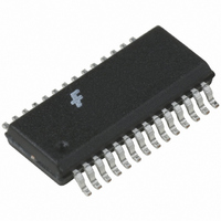
FAN5236QSCX Fairchild Semiconductor, FAN5236QSCX Datasheet - Page 16

FAN5236QSCX
Manufacturer Part Number
FAN5236QSCX
Description
IC CTRLR DDR/PWM DUAL HE 28QSOP
Manufacturer
Fairchild Semiconductor
Datasheet
1.FAN5236MTCX.pdf
(19 pages)
Specifications of FAN5236QSCX
Applications
Controller, Mobile-Friendly DDR
Voltage - Input
5 ~ 24 V
Number Of Outputs
2
Voltage - Output
0.9 ~ 5 V
Operating Temperature
-10°C ~ 85°C
Mounting Type
Surface Mount
Package / Case
28-QSOP
Operating Temperature Range
- 10 C to + 85 C
Mounting Style
SMD/SMT
Lead Free Status / RoHS Status
Lead free / RoHS Compliant
Other names
FAN5236QSCXTR
FAN5236QSCX_NL
FAN5236QSCX_NLTR
FAN5236QSCX_NLTR
FAN5236QSCX_NL
FAN5236QSCX_NLTR
FAN5236QSCX_NLTR
Available stocks
Company
Part Number
Manufacturer
Quantity
Price
Company:
Part Number:
FAN5236QSCX
Manufacturer:
FAIRCHIL
Quantity:
17 500
Part Number:
FAN5236QSCX
Manufacturer:
FAIRCHILD/仙童
Quantity:
20 000
© 2002 Fairchild Semiconductor Corporation
FAN5236 • Rev. 1.3.2
Dual Converter 180° Phased
In dual mode (shown in Figure 6), both converters
contribute to the capacitor input ripple current. With
each converter operating 180° out of phase, the RMS
currents add in the following fashion:
which, for the dual 3A converters shown in Figure 6,
calculates to:
Power MOSFET Selection
Losses in a MOSFET are the sum of its switching (P
and conduction (P
In typical applications, the FAN5236 converter’s output
voltage is low with respect to its input voltage.
Therefore, the lower MOSFET (Q2) is conducting the
full load current for most of the cycle. Q2 should
therefore be selected to minimize conduction losses,
thereby selecting a MOSFET with low R
In contrast, the high-side MOSFET (Q1) has a shorter
duty cycle and it’s conduction loss has less impact. Q1,
however, sees most of the switching losses, so Q1’s
primary selection criteria should be gate charge.
High-Side Losses
Figure 17 shows a MOSFET’s switching interval, with
the upper graph being the voltage and current on the
drain-to-source and the lower graph detailing V
time with a constant current charging the gate. The X-
axis, therefore, is also representative of gate charge
(Q
timing. C
during t3 (as V
parameters on the lower graph are either specified or
can be derived from MOSFET datasheets.
Assuming switching losses are about the same for both
the rising edge and falling edge, Q1’s switching losses
occur during the shaded time when the MOSFET has
voltage across it and current through it.
These losses are given by:
I
I
I
P
P
P
RMS
RMS
RMS
UPPER
SW
COND
G
). C
=
=
=
=
=
⎛
⎜
⎜
⎝
ISS
=
V
1
V
GD
V
4 .
P
( )
DS
I
OUT
I
= C
IN
RMS
1
SW
2
A
receives the current from the gate driver
×
2
I
×
(
GD
+
L
D
(
I
) 1
DS
P
OUT
×
1
COND
COND
2
+ C
2
−
2
+
is falling). The gate charge (Q
×
D
×
t
I
) losses.
GS
1
s
RMS
R
2
⎞
⎟
⎟
⎠
)
DS
and it controls t1, t2, and t4
f
+
SW
(
(
ON
) 2
( )
I
2
)
2
2
or
(
D
2
−
DS(ON)
D
2
2
)
.
(24)
(25)
(26)
(27)
(28)
(29)
GS
vs.
SW
G
)
)
16
P
and P
given MOSFET. R
temperature (T
time), shown as t2+t3 in Figure 17.
The driver’s impedance and C
t3’s period is controlled by the driver’s impedance and
Q
constant current assumption for the driver to simplify
the calculation of t
Most MOSFET vendors specify Q
can be determined as:
where Q
MOSFET to its threshold (V
Q
t
s
UPPER
GD
V
G
V
V
=
DS
(
V
I
TH
GS
. Since most of t
SW
D
SP
Q
I
COND
DRIVER
G
)
is the upper MOSFET’s total losses and P
Figure 17.
5V
(
Figure 18.
SW
=
TH
R
Q
are the switching and conduction losses for a
D
)
GD
t1
=
is the gate charge required to get the
C
Q
ISS
⎛
⎜
⎜
⎝
J
+
). t
GS
R
Q
DRIVER
S
GS
S
V
t2
:
DS(ON)
Q
CC
is the switching period (rise or fall
Switching Losses and Q
S
Drive Equivalent Circuit
Q
SW
−
HDRV
G
−
(
Q
G(SW)
occurs when V
SW
+
V
TH
R
C
is at the maximum junction
)
SP
Q
TH
GATE
GD
GD
t3
).
G
⎞
⎟
⎟
⎠
ISS
R
GATE
GD
determine t2, while
C
t4
GS
C
C
and Q
GD
GS
ISS
= V
www.fairchildsemi.com
t5
4.5V
VIN
GS.
SP
G
, use a
(31)
Q
(30)
G(SW)
SW


