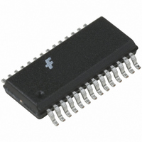
FAN5236QSCX Fairchild Semiconductor, FAN5236QSCX Datasheet - Page 15

FAN5236QSCX
Manufacturer Part Number
FAN5236QSCX
Description
IC CTRLR DDR/PWM DUAL HE 28QSOP
Manufacturer
Fairchild Semiconductor
Datasheet
1.FAN5236MTCX.pdf
(19 pages)
Specifications of FAN5236QSCX
Applications
Controller, Mobile-Friendly DDR
Voltage - Input
5 ~ 24 V
Number Of Outputs
2
Voltage - Output
0.9 ~ 5 V
Operating Temperature
-10°C ~ 85°C
Mounting Type
Surface Mount
Package / Case
28-QSOP
Operating Temperature Range
- 10 C to + 85 C
Mounting Style
SMD/SMT
Lead Free Status / RoHS Status
Lead free / RoHS Compliant
Other names
FAN5236QSCXTR
FAN5236QSCX_NL
FAN5236QSCX_NLTR
FAN5236QSCX_NLTR
FAN5236QSCX_NL
FAN5236QSCX_NLTR
FAN5236QSCX_NLTR
Available stocks
Company
Part Number
Manufacturer
Quantity
Price
Company:
Part Number:
FAN5236QSCX
Manufacturer:
FAIRCHIL
Quantity:
17 500
Part Number:
FAN5236QSCX
Manufacturer:
FAIRCHILD/仙童
Quantity:
20 000
© 2002 Fairchild Semiconductor Corporation
FAN5236 • Rev. 1.3.2
Design and Component Selection Guidelines
As an initial step, define operating input voltage range,
output voltage, and minimum and maximum load
currents for the controller.
Setting the Output Voltage
The internal reference voltage is 0.9V. The output is
divided down by a voltage divider to the VSEN pin (for
example, R5 and R6 in Figure 5). The output voltage
therefore is:
To minimize noise pickup on this node, keep the
resistor to GND (R6) below 2K; for example, R6 at
1.82KΩ. Then choose R5:
For DDR applications converting from 3.3V to 2.5V or
other applications requiring high duty cycles, the duty
cycle clamp must be disabled by tying the converter’s
FPWM to GND. When converter’s FPWM is at GND,
the converter’s maximum duty cycle is greater than
90%. When using as a DDR converter with 3.3V input,
set up the converter for in-phase synchronization by
tying the VIN pin to +5V.
Output Inductor Selection
The minimum practical output inductor value keeps
inductor current just on the boundary of continuous
conduction at some minimum load. The industry
standard practice is to choose the minimum current
somewhere from 15% to 35% of the nominal current. At
light load, the controller can automatically switch to
Hysteretic Mode of operation to sustain high efficiency.
The following equations help to choose the proper value
of the output filter inductor:
where ΔI is the inductor ripple current and ΔV
maximum ripple allowed:
for this example, use:
therefore:
R
L
Δ
f
L ≈
Δ
V
0
SW
R
9 .
I
I
IN
5
=
6
=
=
V
=
=
=
6
V
20
2
=
(
µH
. 1
20
IN
f
300
×
SW
%
V
82
1
V ,
−
OUT
MIN
•
KHz
K
×
V
6
OUT
R
Ω
A
−
OUT
Δ
5
=
)
0
0
I
(
V
=
9 .
9 .
=
Δ
OUT
1
ESR
V
V
×
2
2 .
OUT
5 .
V
A
−
V
OUT
0
IN
9 .
)
=
. 3
24
K
OUT
(12)
(13)
(14)
(15)
(16)
(17)
is the
15
Output Capacitor Selection
The output capacitor serves two major functions in a
switching power supply. Along with the inductor, it filters
the sequence of pulses produced by the switcher and it
supplies the load transient currents. The output
capacitor requirements are usually dictated by ESR,
inductor ripple current (ΔI), and the allowable ripple
voltage (ΔV):
In addition, the capacitor’s ESR must be low enough to
allow the converter to stay in regulation during a load
step. The ripple voltage due to ESR for the converter in
Figure 6 is 120mV
due to the capacitance value itself:
which is only about 1.5mV, for the converter in Figure 6,
and can be ignored.
The capacitor must also be rated to withstand the RMS
current, which is approximately 0.3 X (ΔI), or about
400mA for the converter in Figure 6. High-frequency
decoupling capacitors should be placed as close to the
loads as physically possible
Input Capacitor Selection
The input capacitor should be selected by its ripple
current rating.
Two-Stage Converter Case
In DDR Mode (shown in Figure 5), the V
is powered by the V
capacitor ripple current is produced by the V
converter. A conservative estimate of the output current
required for the 2.5V regulator is:
As an example, if the average I
I
voltage is 16V, RMS input ripple current is:
where D is the duty cycle of the PWM1 converter:
therefore:
ESR
I
I
D
I
Δ
VTT
RMS
REGI
RMS
V
<
is 1A, I
=
V
=
=
<
V
=
C
OUT
I
I
IN
3
Δ
OUT
OUT
VDDQ
Δ
5 .
V
I
(
=
VDDQ
MAX
2
16
×
2
Δ
+
16
5 .
8
5 .
I
)
I
×
VTT
current is about 3.5A. If average input
−
2
D
f
⎛
⎜
⎜
⎝
SW
PP
DDQ
−
2
16
. Some additional ripple appears
5 .
D
output; therefore, all of the input
2
⎞
⎟
⎟
⎠
2
.
=
. 1
VDDQ
49
A
is 3A and average
TT
power input
www.fairchildsemi.com
(18)
(19)
(20)
(21)
(22)
(23)
DDQ


