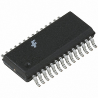
FAN5236QSCX Fairchild Semiconductor, FAN5236QSCX Datasheet - Page 10

FAN5236QSCX
Manufacturer Part Number
FAN5236QSCX
Description
IC CTRLR DDR/PWM DUAL HE 28QSOP
Manufacturer
Fairchild Semiconductor
Datasheet
1.FAN5236MTCX.pdf
(19 pages)
Specifications of FAN5236QSCX
Applications
Controller, Mobile-Friendly DDR
Voltage - Input
5 ~ 24 V
Number Of Outputs
2
Voltage - Output
0.9 ~ 5 V
Operating Temperature
-10°C ~ 85°C
Mounting Type
Surface Mount
Package / Case
28-QSOP
Operating Temperature Range
- 10 C to + 85 C
Mounting Style
SMD/SMT
Lead Free Status / RoHS Status
Lead free / RoHS Compliant
Other names
FAN5236QSCXTR
FAN5236QSCX_NL
FAN5236QSCX_NLTR
FAN5236QSCX_NLTR
FAN5236QSCX_NL
FAN5236QSCX_NLTR
FAN5236QSCX_NLTR
Available stocks
Company
Part Number
Manufacturer
Quantity
Price
Company:
Part Number:
FAN5236QSCX
Manufacturer:
FAIRCHIL
Quantity:
17 500
Part Number:
FAN5236QSCX
Manufacturer:
FAIRCHILD/仙童
Quantity:
20 000
© 2002 Fairchild Semiconductor Corporation
FAN5236 • Rev. 1.3.2
Circuit Description
Overview
The FAN5236 is a multi-mode, dual-channel PWM
controller intended for graphic chipset, SDRAM, DDR
DRAM, or other low-voltage power applications in
modern notebook, desktop, and sub-notebook PCs.
The IC integrates control circuitry for two synchronous
buck converters. The output voltage of each controller
can be set in the range of 0.9V to 5.5V by an external
resistor divider.
The two synchronous buck converters can operate from
either an unregulated DC source (such as a notebook
battery), with voltage ranging from 5.0V to 24V, or from
a regulated system rail of 3.3V to 5.0V. In either mode,
the IC is biased from a +5V source. The PWM
modulators use an average-current-mode control with
input voltage feedforward for simplified feedback loop
compensation and improved line regulation. Both PWM
controllers have integrated feedback loop compensation
that reduces the external components needed.
Depending on the load level, the converters can
operate in fixed-frequency PWM Mode or in a Hysteretic
Mode. Switch-over from PWM to Hysteretic Mode
improves the converters’ efficiency at light loads and
prolongs
comparators are synchronized to the main clock, which
allows seamless transition between the modes and
reduces channel-to-channel interaction. The Hysteretic
Mode can be inhibited independently for each channel if
variable frequency operation is not desired.
The FAN5236 can be configured to operate as a
complete DDR solution. When the DDR pin is set HIGH,
the second channel provides the capability to track the
output voltage of the first channel. The PWM2 converter
is prevented from going into Hysteretic Mode if the DDR
pin is set HIGH. In DDR Mode, a buffered reference
voltage (buffered voltage of the REF2 pin), required by
DDR memory chips, is provided by the PG2 pin.
Converter Modes and Synchronization
Table 3. Converter Modes and Synchronization
When used as a dual converter, as shown in Figure 6,
out-of-phase operation with 180-degree phase shift
reduces input current ripple.
For “two-step” conversion (where the V
from V
cycle of the second converter is nominally 50% and the
optimal phasing depends on V
keep noise generated from the switching transition in
one converter from influencing the "decision" to switch
in the other converter.
Mode
DDR1
DDR2
DUAL
DDQ
Battery
as in Figure 5) used in DDR Mode, the duty
battery
ANY
+5V
V
IN
R to GND
VIN Pin
run
V
V
IN
IN
time.
DDR
HIGH
HIGH
LOW
Pin
IN
In
. The objective is to
Hysteretic
PWM 2 w.r.t.
TT
IN PHASE
is converted
PWM1
+180°
+90°
Mode,
10
When V
7.5V. As shown in Figure 7, 180° operation is
undesirable because the turn-on of the V
occurs very near the decision point of the V
In-phase operation is optimal to reduce inter-converter
interference when V
from a battery), as shown in Figure 8. Because the duty
cycle of PWM1 (generating V
point occurs far away from the decision point for the V
regulator, whose duty cycle is nominally 50%.
When V
rejected for the reasons demonstrated in Figure 7.
In-phase operation with V
the switch point of either converter occurs near the
switch point of the other converter, as seen in Figure 9.
In this case, as V
cause early termination of the V
Conversely, the V
termination of the V
lower than 5V.
These problems are solved by delaying the second
converter’s clock by 90°, as shown in Figure 10. In this
way, all switching transitions in one converter take place
far away from the decision points of the other converter.
Figure 7. Noise-Susceptible 180° Phasing for DDR1
Figure 9.
Figure 8. Optimal In-Phase Operation for DDR1
V
V
V
V
D DQ
V
V
DDQ
DDQ
V
DDQ
V
CLK
CLK
TT
CLK
CLK
TT
TT
TT
Figure 10. Optimal 90° Phasing for DDR2
IN
IN
is from the battery, it’s typically higher than
≈ 5V, 180° phase-shifted operation can be
Noise-Susceptible In-Phase Operation
IN
TT
is a little higher than 5V, it tends to
DDQ
IN
is higher than 5V (when V
switch point can cause early
pulse width when V
for DDR2
IN
≈ 5V is even worse, since
DDQ
) is short, the switching
TT
DDQ
pulse width.
TT
www.fairchildsemi.com
IN
converter.
converter
is slightly
IN
TT
is


