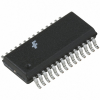
FAN5236QSCX Fairchild Semiconductor, FAN5236QSCX Datasheet - Page 11

FAN5236QSCX
Manufacturer Part Number
FAN5236QSCX
Description
IC CTRLR DDR/PWM DUAL HE 28QSOP
Manufacturer
Fairchild Semiconductor
Datasheet
1.FAN5236MTCX.pdf
(19 pages)
Specifications of FAN5236QSCX
Applications
Controller, Mobile-Friendly DDR
Voltage - Input
5 ~ 24 V
Number Of Outputs
2
Voltage - Output
0.9 ~ 5 V
Operating Temperature
-10°C ~ 85°C
Mounting Type
Surface Mount
Package / Case
28-QSOP
Operating Temperature Range
- 10 C to + 85 C
Mounting Style
SMD/SMT
Lead Free Status / RoHS Status
Lead free / RoHS Compliant
Other names
FAN5236QSCXTR
FAN5236QSCX_NL
FAN5236QSCX_NLTR
FAN5236QSCX_NLTR
FAN5236QSCX_NL
FAN5236QSCX_NLTR
FAN5236QSCX_NLTR
Available stocks
Company
Part Number
Manufacturer
Quantity
Price
Company:
Part Number:
FAN5236QSCX
Manufacturer:
FAIRCHIL
Quantity:
17 500
Part Number:
FAN5236QSCX
Manufacturer:
FAIRCHILD/仙童
Quantity:
20 000
© 2002 Fairchild Semiconductor Corporation
FAN5236 • Rev. 1.3.2
V
V
Initialization and Soft Start
Assuming EN is HIGH, FAN5236 is initialized when V
exceeds the rising UVLO threshold. Should V
below the UVLO threshold, an internal power-on reset
function disables the chip.
The voltage at the positive input of the error amplifier is
limited by the voltage at the SS pin, which is charged
with a 5μA current source. Once C
V
it takes SS to reach 0.9V is:
where t
When SS reaches 1.5V, the power-good outputs are
enabled and Hysteretic Mode is allowed. The converter
is forced into PWM Mode during soft-start.
Operation Mode Control
The mode-control circuit changes the converter mode
from PWM to hysteretic and vice versa, based on the
voltage polarity of the SW node when the lower
MOSFET is conducting and just before the upper
MOSFET turns on. For continuous inductor current, the
SW node is negative when the lower MOSFET is
conducting and the converters operate in fixed-
Hysteretic Mode
Conversely, the transition from Hysteretic Mode to
PWM Mode occurs when the SW node is negative for
eight consecutive cycles.
A sudden increase in the output current causes a
change from Hysteretic to PWM Mode. This load
increase causes an instantaneous decrease in the
output voltage due to the voltage drop on the output
capacitor ESR. If the load causes the output voltage (as
presented at V
regulation level (20mV below V
changed to PWM on the next clock cycle.
In Hysteretic Mode, the PWM comparator and the error
amplifier that provide control in PWM Mode are
inhibited and the hysteretic comparator is activated. In
Hysteretic Mode, the low-side MOSFET is operated as
a synchronous rectifier, where the voltage across
t
CORE
CORE
0
REF
9 .
I
I
L
L
=
(0.9V) the output voltage is in regulation. The time
0
0
0
0.9
9 .
xC
5
is in seconds if C
SS
SNS
) to drop below the hysteretic
Figure 11.
SS
is in μF.
1
REF
PWMMode
SS
Transitioning Between PWM and Hysteretic Mode
), the mode is
2
has charged to
1
2
HystereticMode
CC
3
drop
3
(1)
CC
4
11
4
frequency PWM Mode, as shown in Figure 11. This
mode achieves high efficiency at nominal load. When
the load current decreases to the point where the
inductor current flows through the lower MOSFET in the
‘reverse’ direction, the SW node becomes positive and
the mode is changed to hysteretic, which achieves
higher efficiency at low currents by decreasing the
effective switching frequency.
To prevent accidental mode change or "mode chatter,"
the transition from PWM to Hysteretic Mode occurs
when the SW node is positive for eight consecutive
clock cycles, as shown in Figure 11. The polarity of the
SW node is sampled at the end of the lower MOSFET
conduction time. At the transition between PWM and
Hysteretic Mode, the upper and lower MOSFETs are
turned off. The phase node “rings” based on the output
inductor and the parasitic capacitance on the phase
node and settles out at the value of the output voltage.
The boundary value of inductor current, where current
becomes discontinuous, can be estimated by the
following expression:
V
positive (current flowing back from the load), allowing
the diode to block reverse conduction.
The hysteretic comparator initiates a PFM signal to turn
on HDRV at the rising edge of the next oscillator clock,
when the output voltage (at V
threshold (10mV below V
signal or when V
(5mV above V
a function of:
I
5
LOAD
DS(ON)
Spread between the two hysteretic thresholds
I
Output inductor and capacitor ESR.
(
LOAD
DIS
6
is monitored and switched off when V
)
5
=
7
⎛
⎜
⎜
⎜
⎝
V (
2
IN
REF
F
8
SW
−
6
). The switching frequency is primarily
V
L
SNS
HystereticMode
OUT
OUT
V
rises over the higher threshold
V )
IN
OUT
REF
7
⎞
⎟
⎟
⎟
⎠
) and terminates the PFM
SNS
) falls below the lower
8
PWMMode
www.fairchildsemi.com
DS(ON)
goes
(2)


