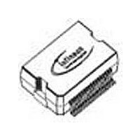
TLE6230GP Infineon Technologies, TLE6230GP Datasheet - Page 9

TLE6230GP
Manufacturer Part Number
TLE6230GP
Description
IC SW SMART OCTAL LOWSIDE PDSO36
Manufacturer
Infineon Technologies
Type
Low Sider
Datasheet
1.TLE6230GP.pdf
(16 pages)
Specifications of TLE6230GP
Input Type
SPI
Number Of Outputs
8
On-state Resistance
800 mOhm
Current - Peak Output
1.5A
Voltage - Supply
4.5 V ~ 5.5 V
Operating Temperature
-40°C ~ 150°C
Mounting Type
Surface Mount
Package / Case
DSO-36
Switch Type
Low Side
Power Switch Family
TLE6230
Input Voltage
-0.3 to 7V
Power Switch On Resistance
800mOhm
Output Current
1A
Mounting
Surface Mount
Supply Current
1mA
Package Type
DSO
Operating Temperature (min)
-40C
Operating Temperature (max)
150C
Operating Temperature Classification
Automotive
Pin Count
38
Power Dissipation
3300W
Packages
PG-DSO-36
Thermal Class
Heatslug down
Id Nom
8 x 0.5 A
Channels
8.0
Comment
relay driver and general purpose
Lead Free Status / RoHS Status
Lead free / RoHS Compliant
Current - Output / Channel
-
Lead Free Status / Rohs Status
Compliant
Other names
SP000012169
SP000691114
TLE6230GP
TLE6230GPNT
TLE6230GPT
TLE6230GPT
TLE6230GPTR
SP000691114
TLE6230GP
TLE6230GPNT
TLE6230GPT
TLE6230GPT
TLE6230GPTR
Available stocks
Company
Part Number
Manufacturer
Quantity
Price
Company:
Part Number:
TLE6230GP
Manufacturer:
INFINEON
Quantity:
1 210
Company:
Part Number:
TLE6230GP
Manufacturer:
INFINEON
Quantity:
804
Part Number:
TLE6230GP
Manufacturer:
INFINEON/英飞凌
Quantity:
20 000
high level at this pin (within the data byte) will switch on the power switch, provided that the
corresponding parallel input is also switched on (AND-operation for channel 1 to 4).
SO - Serial Output. Diagnostic data bits are shifted out serially at this pin, the most significant
bit first. SO is in a high impedance state until the CS pin goes to a logic low state. New diag-
nostic data will appear at the SO pin following the rising edge of SCLK.
switches all outputs OFF. An internal pull-up structure is provided on chip.
Diagnostics
tion as soon as an error occurs for any one of the eight channels. This fault indication can be
used to generate a µC interrupt. Therefore a ‘diagnosis’ interrupt routine need only be called
after this fault indication. This saves processor time compared to a cyclic reading of the SO
information.
As soon as a fault occurs, the fault information is latched into the diagnosis register. A new
error will over-write the old error report. Serial data out pin (SO) is in a high impedance state
when CS is high. If CS receives a LOW signal, all diagnosis bits can be shifted out serially.
The rising edge of CS will reset all error registers.
There are two diagnostic bits per channel configured as shown in Figure 1.
Normal function: The bit combination HH indicates that there is no fault condition, i.e. normal
function.
Overload, Short Circuit to Battery (SCB) or Overtemperature: HL is set when the current
limitation gets active, i.e. there is a overload, short to supply or overtemperature condition.
Open load: An open load condition is detected when the drain voltage decreases below 3 V
(typ.). LH bit combination is set.
Short Circuit to GND: If a drain to ground short circuit exists and the drain to ground current
exceeds 100 µA, short to ground is detected and the LL bit combination is set.
V2.3
Figure 1: Two bits per channel diagnostic feedback
RESET
FAULT
Diagnostic Serial Data Out SO
HH
HL
LH
LL
- Reset pin. If the reset pin is in a logic low state, it clears the SPI shift register and
- Fault pin. There is a general fault pin (open drain) which shows a high to low transi-
15
Ch.8
14
Normal function
Overload, Shorted Load or Overtemperature
Open Load
Shorted to Ground
13
Ch.7
12
11 10
Ch.6
9
Ch.5
8
Page
- - - - -
9
Data Sheet TLE 6230 GP
18. Nov. 2009


