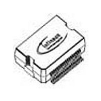
TLE6230GP Infineon Technologies, TLE6230GP Datasheet - Page 7

TLE6230GP
Manufacturer Part Number
TLE6230GP
Description
IC SW SMART OCTAL LOWSIDE PDSO36
Manufacturer
Infineon Technologies
Type
Low Sider
Datasheet
1.TLE6230GP.pdf
(16 pages)
Specifications of TLE6230GP
Input Type
SPI
Number Of Outputs
8
On-state Resistance
800 mOhm
Current - Peak Output
1.5A
Voltage - Supply
4.5 V ~ 5.5 V
Operating Temperature
-40°C ~ 150°C
Mounting Type
Surface Mount
Package / Case
DSO-36
Switch Type
Low Side
Power Switch Family
TLE6230
Input Voltage
-0.3 to 7V
Power Switch On Resistance
800mOhm
Output Current
1A
Mounting
Surface Mount
Supply Current
1mA
Package Type
DSO
Operating Temperature (min)
-40C
Operating Temperature (max)
150C
Operating Temperature Classification
Automotive
Pin Count
38
Power Dissipation
3300W
Packages
PG-DSO-36
Thermal Class
Heatslug down
Id Nom
8 x 0.5 A
Channels
8.0
Comment
relay driver and general purpose
Lead Free Status / RoHS Status
Lead free / RoHS Compliant
Current - Output / Channel
-
Lead Free Status / Rohs Status
Compliant
Other names
SP000012169
SP000691114
TLE6230GP
TLE6230GPNT
TLE6230GPT
TLE6230GPT
TLE6230GPTR
SP000691114
TLE6230GP
TLE6230GPNT
TLE6230GPT
TLE6230GPT
TLE6230GPTR
Available stocks
Company
Part Number
Manufacturer
Quantity
Price
Company:
Part Number:
TLE6230GP
Manufacturer:
INFINEON
Quantity:
1 210
Company:
Part Number:
TLE6230GP
Manufacturer:
INFINEON
Quantity:
804
Part Number:
TLE6230GP
Manufacturer:
INFINEON/英飞凌
Quantity:
20 000
Functional Description
The TLE 6230 GP is an octal-low-side power switch which provides a serial peripheral inter-
face (SPI) to control the 8 power DMOS switches, as well as diagnostic feedback. The power
transistors are protected against short to V
voltage by an active zener clamp.
The diagnostic logic recognizes a fault condition which can be read out via the serial diagnostic
output (SO).
Circuit Description
Output Stage Control
Each output is independently controlled by an output latch and a common reset line, which
disables all eight outputs. Serial data input (SI) is read on the falling edge of the serial clock. A
logic high input data bit turns the respective output channel ON, a logic low data bit turns it
OFF. CS must be low whilst shifting all the serial data into the device. A low-to-high transition
of CS transfers the serial data input bits to the output buffer.
Special conditions for Channel 1 to 4:
In addition to the serial control of the outputs it is possible to control channel 1 to channel 4
directly in parallel for PWM applications. These inputs are high or low active (programmable
via PRG pin) and ANDed with the SPI control bit.
The table shows the AND-operation of the parallel
input pin (here active high) and the corresponding
SPI bit. For an application where the parallel input is
always "ON", it is possible to switch the channel
OFF via the SPI bit, e.g. for diagnosis in OFF-state.
⇒ SPI Priority for OFF-state
Operation with parallel inputs: Set SPI bits to logic high.
Operation via SPI: Connect parallel inputs to logic high (if programmed to active high).
PRG - Program pin.
If the parallel input pins are not connected (independent of high or low activity) it is guaranteed
that the channels 1 to 4 are switched OFF.
PRG pin itself is internally pulled up when it is not connected.
V2.3
PRG = High (V
PRG = Low (GND): Parallel inputs Channel 1 to 4 are low active.
S
):
Page
Parallel inputs Channel 1 to 4 are high active
BB
, overload, overtemperature and against over-
7
IN 1 - 4
0
0
1
1
Data Sheet TLE 6230 GP
SPI-Bit 0 - 3
0
1
0
1
18. Nov. 2009
OUT 1 - 4
OFF
OFF
OFF
ON


