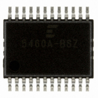
CS5460A-BSZ Cirrus Logic Inc, CS5460A-BSZ Datasheet - Page 45

CS5460A-BSZ
Manufacturer Part Number
CS5460A-BSZ
Description
IC ENERGY METERING 1PHASE 24SSOP
Manufacturer
Cirrus Logic Inc
Datasheet
1.CS5460A-BSZ.pdf
(54 pages)
Specifications of CS5460A-BSZ
Package / Case
24-SSOP
Input Impedance
30 KOhm
Measurement Error
0.1%
Voltage - I/o High
0.8V
Voltage - I/o Low
0.2V
Current - Supply
2.9mA
Voltage - Supply
4.75 V ~ 5.25 V
Operating Temperature
-40°C ~ 85°C
Mounting Type
Surface Mount
Meter Type
Single Phase
Output Voltage Range
2.4 V to 2.6 V
Output Current
1 uA
Input Voltage Range
2.4 V to 2.6 V
Input Current
25 nA
Power Dissipation
500 mW
Operating Temperature Range
- 40 C to + 85 C
Mounting Style
SMD/SMT
Ic Function
Single Phase Bi-directional Power / Energy IC
Brief Features
On-Chip Functions, AC Or DC System Calibration, Power Supply Monitor
Supply Voltage Range
3.3V To 5V
Rohs Compliant
Yes
Lead Free Status / RoHS Status
Lead free / RoHS Compliant
For Use With
CDB5460AU - EVALUATION BOARD FOR CS5460A
Lead Free Status / Rohs Status
Lead free / RoHS Compliant
Other names
598-1094-5
Available stocks
Company
Part Number
Manufacturer
Quantity
Price
Company:
Part Number:
CS5460A-BSZ
Manufacturer:
CIRRUS
Quantity:
2
Company:
Part Number:
CS5460A-BSZR
Manufacturer:
CIRRUS
Quantity:
8 000
Part Number:
CS5460A-BSZR
Manufacturer:
CIRRUS
Quantity:
20 000
DS487F4
Res
EWA
Gi
PC[6:0]
RS
DL0
DL1
EOD
SI[1:0]
automatically returned to 0 by the reset cycle.
Default = '0'
Default = '0'
also be accessed using the Status Register.
0 = Normal operation of the EOUT and EDIR pins. (default)
1 = DL0 and DL1 bits control the EOUT and EDIR pins.
00 = active low level (default)
01 = active high level
10 = falling edge (INT is normally high)
11 = rising edge (INT is normally low)
ing an external pull-up device.
0 = normal outputs (default)
1 = only the pull-down device of the EOUT and EDIR pins are active
0 = gain is 10 (default)
1 = gain is 50
When MCLK = 4.096 MHz and K = 1, the phase adjustment range is about -2.8 to +2.8 degrees
and each step is about 0.04 degrees (this assumes that the power line frequency is 60 Hz). If
(MCLK / K) is not 4.096 MHz, the values for the range and step size should be scaled by the
factor 4.096 MHz / (MCLK / K).
Default setting is 0000000 = 0.0215 degrees phase delay (when MCLK = 4.096 MHz).
Start a chip reset cycle when set 1. The reset cycle lasts for less than 10 XIN cycles. The bit is
When EOD = 1, EDIR becomes a user defined pin. DL0 sets the value of the EDIR pin.
When EOD = 1, EOUT becomes a user defined pin. DL1 sets the value of the EOUT pin.
Allows the EOUT and EDIR pins to be controlled by the DL0 and DL1 bits. EOUT and EDIR can
Soft interrupt configuration. Select the desired pin behavior for indication of an interrupt.
Reserved. These bits must be set to zero.
Allows the output pins of EOUT and EDIR of multiple chips to be connected in a wire-AND, us-
Sets the gain of the current PGA
Phase compensation. A 2’s complement number used to set the delay in the voltage channel.
CS5460A
45


