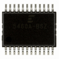
CS5460A-BSZ Cirrus Logic Inc, CS5460A-BSZ Datasheet - Page 31

CS5460A-BSZ
Manufacturer Part Number
CS5460A-BSZ
Description
IC ENERGY METERING 1PHASE 24SSOP
Manufacturer
Cirrus Logic Inc
Datasheet
1.CS5460A-BSZ.pdf
(54 pages)
Specifications of CS5460A-BSZ
Package / Case
24-SSOP
Input Impedance
30 KOhm
Measurement Error
0.1%
Voltage - I/o High
0.8V
Voltage - I/o Low
0.2V
Current - Supply
2.9mA
Voltage - Supply
4.75 V ~ 5.25 V
Operating Temperature
-40°C ~ 85°C
Mounting Type
Surface Mount
Meter Type
Single Phase
Output Voltage Range
2.4 V to 2.6 V
Output Current
1 uA
Input Voltage Range
2.4 V to 2.6 V
Input Current
25 nA
Power Dissipation
500 mW
Operating Temperature Range
- 40 C to + 85 C
Mounting Style
SMD/SMT
Ic Function
Single Phase Bi-directional Power / Energy IC
Brief Features
On-Chip Functions, AC Or DC System Calibration, Power Supply Monitor
Supply Voltage Range
3.3V To 5V
Rohs Compliant
Yes
Lead Free Status / RoHS Status
Lead free / RoHS Compliant
For Use With
CDB5460AU - EVALUATION BOARD FOR CS5460A
Lead Free Status / Rohs Status
Lead free / RoHS Compliant
Other names
598-1094-5
Available stocks
Company
Part Number
Manufacturer
Quantity
Price
Company:
Part Number:
CS5460A-BSZ
Manufacturer:
CIRRUS
Quantity:
2
Company:
Part Number:
CS5460A-BSZR
Manufacturer:
CIRRUS
Quantity:
8 000
Part Number:
CS5460A-BSZR
Manufacturer:
CIRRUS
Quantity:
20 000
3.8.7.2 DC Offset Calibration Sequence
The Voltage Channel DC Offset Register holds the
negative of the simple average of N samples taken
while the DC voltage offset calibration was execut-
ed. The inputs should be grounded during DC off-
set calibration. The DC offset value is added to the
signal path to nullify the DC offset in the system.
3.8.7.3 AC Gain Calibration Sequence
The AC voltage gain calibration algorithm attempts
to adjust the Voltage Channel Gain Register value
such that the calibration reference signal level pre-
sented at the voltage inputs will result in a value of
0.6 in the RMS Voltage Register. The AC calibra-
tion signal is applied to the “+” and “-” input pins of
the channel under calibration. During AC voltage
gain calibration, the value in the RMS Voltage Reg-
ister is divided into 0.6. This result is the AC gain
calibration value stored in the Voltage Channel
Gain Register.
3.8.7.4 DC Gain Calibration Sequence
Based on the level of the positive DC calibration
voltage that should be applied across the “+” and
“-” inputs, the CS5460A determines the Voltage
Channel Gain Register value by averaging the In-
stantaneous Voltage Register’s output signal val-
DS487F4
Sinewave
Sinewave
SIGNAL
SIGNAL
INPUT
INPUT
-230 mV
-250 mV
Figure 19. Example of AC Gain Calibration
-230 mV
-250 mV
250 mV
230 mV
250 mV
230 mV
After AC Gain Calibration (Vgain Register changed to ~0.9223)
Before AC Gain Calibration (Vgain Register = 1)
0 V
0 V
V
RMS
V
Register =
RMS
Register = 0.6000...
230
/
250
x
1
/
√2
≈ 0.65054
-1.0000...
-0.84853
-0.92231
0.92231
0.84853
0.9999...
-0.92
0.92
Instantaneous Voltage
Instantaneous Voltage
Register Values
Register Values
ues over one computation cycle (N samples) and
then dividing this average into 1. Therefore, after
the DC voltage gain calibration has been executed,
the Instantaneous Voltage Register will read
full-scale whenever the DC level of the input signal
is equal to the level of the DC calibration signal that
was applied to the voltage channel inputs during
the DC gain calibration. For example, if a +230 mV
DC signal is applied to the voltage channel inputs
during the DC gain calibration for the current chan-
nel, then the Instantaneous Voltage Register will
measure unity whenever a 230 mV DC level is ap-
plied to the voltage channel inputs.
3.8.8 Duration of Calibration Sequence
The value of the Cycle Count Register (N) deter-
mines the number of conversions that will be per-
formed by the CS5460A during a given calibration
sequence. For DC offset/gain calibrations, the cal-
ibration sequence always takes at least N + 30
conversion cycles to complete. For AC offset/gain
calibrations, the calibration sequence takes at
least 6N + 30 A/D conversion cycles to complete,
(about 6 computation cycles). If N is increased, the
accuracy of calibration results will increase.
For more information on Calibration, see AN227,
“CALIBRATING THE CS5460A”.
3.9 Phase Compensation
The values of bits 23 to 17 in the Configuration
Register can be altered to adjust the amount of
time delay that is imposed on the digitally sampled
voltage channel signal. This time delay is applied
to the voltage channel signal in order to compen-
sate for the relative phase delay (with respect to
the fundamental frequency) between the sensed
voltage and current signals. Voltage and current
transformers, as well as other sensor/filter/protec-
tion devices deployed at the front-end of the volt-
age/current sensor networks can often introduce a
phase-delay in the system that distorts/corrupts
the phase relationship between the line-voltage
and line-current signals that are to be measured.
The phase compensation bits PC[6:0] in the Con-
figuration Register can be set to nullify this undesir-
able phase distortion between the digitally
sampled signals in the two channels. The value in
the 7-bit phase compensation word indicates the
amount of time delay that is imposed on the volt-
CS5460A
31


