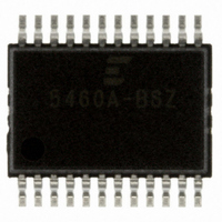
CS5460A-BSZ Cirrus Logic Inc, CS5460A-BSZ Datasheet - Page 32

CS5460A-BSZ
Manufacturer Part Number
CS5460A-BSZ
Description
IC ENERGY METERING 1PHASE 24SSOP
Manufacturer
Cirrus Logic Inc
Datasheet
1.CS5460A-BSZ.pdf
(54 pages)
Specifications of CS5460A-BSZ
Package / Case
24-SSOP
Input Impedance
30 KOhm
Measurement Error
0.1%
Voltage - I/o High
0.8V
Voltage - I/o Low
0.2V
Current - Supply
2.9mA
Voltage - Supply
4.75 V ~ 5.25 V
Operating Temperature
-40°C ~ 85°C
Mounting Type
Surface Mount
Meter Type
Single Phase
Output Voltage Range
2.4 V to 2.6 V
Output Current
1 uA
Input Voltage Range
2.4 V to 2.6 V
Input Current
25 nA
Power Dissipation
500 mW
Operating Temperature Range
- 40 C to + 85 C
Mounting Style
SMD/SMT
Ic Function
Single Phase Bi-directional Power / Energy IC
Brief Features
On-Chip Functions, AC Or DC System Calibration, Power Supply Monitor
Supply Voltage Range
3.3V To 5V
Rohs Compliant
Yes
Lead Free Status / RoHS Status
Lead free / RoHS Compliant
For Use With
CDB5460AU - EVALUATION BOARD FOR CS5460A
Lead Free Status / Rohs Status
Lead free / RoHS Compliant
Other names
598-1094-5
Available stocks
Company
Part Number
Manufacturer
Quantity
Price
Company:
Part Number:
CS5460A-BSZ
Manufacturer:
CIRRUS
Quantity:
2
Company:
Part Number:
CS5460A-BSZR
Manufacturer:
CIRRUS
Quantity:
8 000
Part Number:
CS5460A-BSZR
Manufacturer:
CIRRUS
Quantity:
20 000
age channel’s analog input signal with respect to
the current channel’s analog input signal.
With the default setting, the phase delay on the
voltage channel signal is ~0.995 µs (~0.0215 de-
grees assuming a 60 Hz power signal). With
MCLK = 4.096 MHz and K = 1, the range of the in-
ternal
-2.8 degrees to +2.8 degrees when the input volt-
age/current signals are at 60 Hz. In this condition,
each step of the phase compensation register (val-
ue of one LSB) is ~0.04 degrees. For values of
MCLK other than 4.096 MHz, these values for the
span (-2.8 to +2.8 degrees) and for the step size
(0.04 degrees)
4.096 MHz / (MCLK / K). For power line frequen-
cies other than 60Hz (e.g., 50 Hz), the values of
the range and step size of the PC[6:0] bits can be
determined by converting the above values to
time-domain (seconds), and then computing the
new range and step size (in degrees) with respect
to the new line frequency.
Unlike offset/gain calibration, the CS5460A does
not provide an automated on-chip phase calibra-
tion sequence. To calibrate the phase delay, the
phase compensation bits can be adjusted while the
CS5460A is running in ‘continuous computation
cycles’ data acquisition mode. For example, the
CS5460A can be set up to perform continuous
computations on a purely resistive load (no induc-
tance or capacitance). The PC[6:0] bits can then
be adjusted until the Energy Register value is max-
imized.
3.10 Time-Base Calibration Register
The Time-Base Calibration Register (notated as
“TBC” in Figure 3) is used to compensate for slight
errors in the XIN input frequency. External oscilla-
tors and crystals have certain tolerances. If there is
a concern about improving the accuracy of the
clock for energy measurements, the Time-Base
Calibration Register value can be manipulated to
compensate for the frequency error. Note from Fig-
ure 3 that the TBC Register only affects the value
in the Energy Register.
As an example, if the desired XIN frequency is
4.096 MHz, but during production-level testing,
suppose that the average frequency of the crystal
on a particular board is measured to actually be
4.091 MHz. The ratio of the desired frequency to
32
phase
compensation
should
be
ranges
scaled
from
by
the actual frequency is 4.096 MHz/4.091 MHz =
~1.00122219506. The TBC Register can be set to
1.00122213364 = 0x80280C(h), which is very
close to the desired ratio.
3.11 Power Offset Register
Referring to Figure 3, note the “P
appears just after the power computation. This reg-
ister can be used to offset system power sources
that may be resident in the system, but do not orig-
inate from the power line signal. These sources of
extra energy in the system contribute undesirable
and false offsets to the power/energy measure-
ment results. For example, even after DC offset
and AC offset calibrations have been run on each
channel, when a voltage signal is applied to the
voltage channel inputs and the current channel is
grounded (i.e., there is zero input on the current
channel), the current channel may still register a
very small amount of RMS current caused by leak-
age of the voltage channel input signal into the cur-
rent channel input signal path. Although the
CS5460A has high channel-to-channel crosstalk
rejection, such crosstalk may not totally be elimi-
nated.) If the amount of ‘artificial’ power that might
be induced into the voltage/current channel signals
due to such crosstalk/system noise/etc. can be de-
termined, then the Power Offset Register can be
programmed to nullify the effects of this unwanted
energy.
3.12 Input Protection - Current Limit
In Figures 6, 7, 8, and 9, note the series resistor R
which is connected to the IIN+ input pin. This resis-
tor serves two purposes. First, this resistor func-
tions in coordination with C
low-pass filter. The filter will a) remove any broad-
band noise that is far outside of the frequency
range of interest, and also b) this filter serves as
the anti-aliasing filter, which is necessary to pre-
vent the A/D converter from receiving input signals
whose frequency is higher than one-half of the
sampling frequency (the Nyquist frequency). The
second purpose of this resistor is to provide cur-
rent-limit protection for the Iin+ input pin, in the
event of a power surge or lightning surge. The role
that R
cussed in the Section 3.13. But first the current-lim-
it protection requirements for the Iin+/Iin- and
Vin+/Vin- pins are discussed.
I+
contributes to input filtering will be dis-
Idiff
and/or C
off
” Register that
CS5460A
Idiff
to form a
DS487F4
I+


