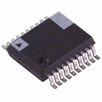
ADE7753ARSZ Analog Devices Inc, ADE7753ARSZ Datasheet - Page 52

ADE7753ARSZ
Manufacturer Part Number
ADE7753ARSZ
Description
IC ENERGY METERING 1PHASE 20SSOP
Manufacturer
Analog Devices Inc
Datasheet
1.ADE7753ARSZ.pdf
(60 pages)
Specifications of ADE7753ARSZ
Input Impedance
390 KOhm
Measurement Error
0.1%
Voltage - I/o High
2.4V
Voltage - I/o Low
0.8V
Current - Supply
3mA
Voltage - Supply
4.75 V ~ 5.25 V
Operating Temperature
-40°C ~ 85°C
Mounting Type
Surface Mount
Package / Case
20-SSOP (0.200", 5.30mm Width)
Meter Type
Single Phase
Ic Function
Single-Phase Multifunction Metering IC
Supply Voltage Range
4.75V To 5.25V
Operating Temperature Range
-40°C To +85°C
Digital Ic Case Style
SSOP
No. Of Pins
20
Lead Free Status / RoHS Status
Lead free / RoHS Compliant
For Use With
EVAL-ADE7753ZEB - BOARD EVALUATION AD7753
Lead Free Status / RoHS Status
Lead free / RoHS Compliant, Lead free / RoHS Compliant
Available stocks
Company
Part Number
Manufacturer
Quantity
Price
Part Number:
ADE7753ARSZ
Manufacturer:
ADI/亚德诺
Quantity:
20 000
Part Number:
ADE7753ARSZRL
Manufacturer:
ADI/亚德诺
Quantity:
20 000
ADE7753
Address
0x12
0x13
0x14
0x15
0x16
0x17
0x18
0x19
0x1A
0x1B
0x1C
0x1D
0x1E
0x1F
0x20
0x21
0x22
0x23
0x24
0x25
0x26
Name
WGAIN
WDIV
CFNUM
CFDEN
IRMS
VRMS
IRMSOS
VRMSOS
VAGAIN
VADIV
LINECYC
ZXTOUT
SAGCYC
SAGLVL
IPKLVL
VPKLVL
IPEAK
RSTIPEAK
VPEAK
RSTVPEAK
TEMP
R/W
R/W
R/W
R/W
R/W
R
R
R/W
R/W
R/W
R/W
R/W
R/W
R/W
R/W
R/W
R/W
R
R
R
R
R
12
8
12
12
24
24
12
12
12
8
16
12
8
8
8
8
24
24
24
24
8
N
o. Bits
Default
0x0
0x0
0x3F
0x3F
0x0
0x0
0x0
0x0
0x0
0x0
0xFFFF
0xFFF
0xFF
0x0
0xFF
0xFF
0x0
0x0
0x0
0x0
0x0
Type
U
U
U
U
U
U
U
U
U
U
U
U
U
U
U
U
S
S
S
S
S
1
Rev. A | Page 52 of 60
Description
Power Gain Adjust. This is a 12-bit register. The active power calculation
can be calibrated by writing to this register. The calibration range is ±50%
of the nomin
0.0244%/LSB —see the Calibrating an Energy Meter Based on the ADE7753
section.
Active Energy Divider Register. The internal active energy register is
divided by the value of this register before being stored in the AENERG
register.
CF Frequency Divider Numerator Register. The output frequency on the CF
pin is adjusted by writing to this 12-bit read/write register—see the
Energy-to-Frequency Conversion section.
CF Frequency Divider Denominator Register. The output frequency on the
CF pin is adjusted by writing to this 12-bit read/write register—see the
Energy-to-Frequency Conversion section.
Channel 1 RMS Value (Current Channel).
Channel 2 RMS Value (Voltage Channel).
Channel 1 RMS Offs
Channel 2 RMS Offset Correction Register.
Apparent Gain Register. App
writing to this register. The calibration range is 50% of the nominal ful
scale real power. The resolution of the gain adjust is 0.02444%/LSB.
Apparent Energy D
divided by the value of this register before being stored in the VAENERGY
register.
Line Cycle Energy A
register is used during line cycle energy accumulation mode to set the
number of half line cycles for energy accumulation—see the Line Cycle
Energy Accumulation Mode section.
Zero-Crossing Timeout. If no zero crossings are detected on
within a time period specified by this 12-bit register, the interrupt request
line (IRQ) is activated—see the Zero-Crossing Detection section.
Sag Line Cycle Register. This 8-bit register specifies the number of
consecutive line cycles the signal on Channel 2 must be below SAGLVL
before th
section.
Sag Voltage Level. An 8-bit write to this register determines at w
signal level on Channel 2 the SAG pin becomes active. The signal must
remain low for the number of cycles specified in the SAGCYC register
before the SAG pin is activated—see the Line Voltage Sag Detection
section.
Channel 1 Peak Level Threshold (Current Channel). This register sets the
level of the current peak detection. If the Channel 1 input exceeds this
level, the PKI flag in the status register is set.
Channel 2 Peak Level Threshold (Voltage Ch
level of the voltage peak detection. If the Channel 2 input exceeds this
level, the PKV flag in the status register is set.
Channel 1 Peak Register. The maximum input value of the current channel
since the last read of the register is stored in this register.
Same as Channel 1 Peak Register except that the register contents are rese
to 0 after read.
Channel 2 Peak Register. The maximum input value of the voltage channel
since the last read of the register is stored in this register.
Same as Channel 2 Peak Register except that the register contents are rese
to 0 after a read.
Temperature Register. This is an 8-bit register which contains the result of
the latest temperature conversion—see the Temperature Measurement
section.
e SAG output is activated—see the Line Voltage Sag Detection
al full-scale active power. The resolution of the gain adjust is
ivider Register. The internal apparent energy register is
et Correction Register.
ccumulation Mode Line-Cycle Register. This 16-bit
arent power calculation can be calibrated by
annel). This register sets the
Channel 2
hat peak
l-
Y
t
t


