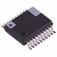
ADE7753ARSZ Analog Devices Inc, ADE7753ARSZ Datasheet - Page 50

ADE7753ARSZ
Manufacturer Part Number
ADE7753ARSZ
Description
IC ENERGY METERING 1PHASE 20SSOP
Manufacturer
Analog Devices Inc
Datasheet
1.ADE7753ARSZ.pdf
(60 pages)
Specifications of ADE7753ARSZ
Input Impedance
390 KOhm
Measurement Error
0.1%
Voltage - I/o High
2.4V
Voltage - I/o Low
0.8V
Current - Supply
3mA
Voltage - Supply
4.75 V ~ 5.25 V
Operating Temperature
-40°C ~ 85°C
Mounting Type
Surface Mount
Package / Case
20-SSOP (0.200", 5.30mm Width)
Meter Type
Single Phase
Ic Function
Single-Phase Multifunction Metering IC
Supply Voltage Range
4.75V To 5.25V
Operating Temperature Range
-40°C To +85°C
Digital Ic Case Style
SSOP
No. Of Pins
20
Lead Free Status / RoHS Status
Lead free / RoHS Compliant
For Use With
EVAL-ADE7753ZEB - BOARD EVALUATION AD7753
Lead Free Status / RoHS Status
Lead free / RoHS Compliant, Lead free / RoHS Compliant
Available stocks
Company
Part Number
Manufacturer
Quantity
Price
Part Number:
ADE7753ARSZ
Manufacturer:
ADI/亚德诺
Quantity:
20 000
Part Number:
ADE7753ARSZRL
Manufacturer:
ADI/亚德诺
Quantity:
20 000
ADE7753
ADE7753 Serial Read Operation
During a data read operation from the ADE7753, data is sh
out at the DOUT logic output on the rising edge of SCLK. As
the case with the data write operation, a data read must be
preceded with a write to the communications register.
With the ADE7753 in communications mode (i.e.,
low), an 8-bit write to the communications register first takes
place. The MSB of this byte transfer is a 0, indicating that the
next data transfer operation is a read. The LSBs of this byte
contain the address of the register that is to be read. The
ADE7753 starts shifting out of the register data on the next
rising edge of SCLK—see Figure 94. At this point, the DOUT
logic output leaves its high impedance state and starts driving
the data bus. All remaining bits of register data are shifted ou
on subsequent SCLK rising edges. The serial interface also
enters communications mode again as soon as the read has
been completed. At this point, the DOUT logic output enters
SCLK
DOUT
DIN
CS
t
1
0
0
A5
COMMAND BYTE
A4
A3
A2
CS logic
Figure 94. Serial Interface Read Timing
A1
ifted
A0
Rev. A | Page 50 of 60
t
a
is
t
t
9
11
DB7
high impedance state on the falling edge of the last SCLK pulse.
The read operation can be aborted by bringing the
input high before the data transfer is complete. The DOUT
output enters a high impedance state on the rising edge of CS .
When an ADE7753 register is addresse
the entire contents of that register are transferred to the s
port. This allows the ADE7753 to modify its on-chip registers
without the risk of corrupting data during a multibyte transf
Note that when a read operation follows a write operation, th
read command (i.e., write to communications register) should
not happen for at least 4 µs after the end of the write operation.
If the read command is sent within 4 µs of the write operation,
the last byte of the write operation could be lost. This timing
constraint is given as timing specification t
MOST SIGNIFICANT BYTE
t
11
DB0
t
10
LEAST SIGNIFICANT BYTE
DB7
d for a read operation,
9
.
t
12
DB0
t
13
CS logic
02875-0-083
erial
er.
e


