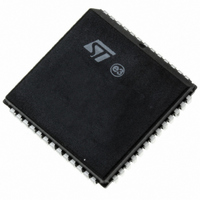
PSD834F2-70J STMicroelectronics, PSD834F2-70J Datasheet - Page 20

PSD834F2-70J
Manufacturer Part Number
PSD834F2-70J
Description
IC FLASH 2MBIT 70NS 52PLCC
Manufacturer
STMicroelectronics
Datasheet
1.PSD813F2VA-20JI.pdf
(109 pages)
Specifications of PSD834F2-70J
Format - Memory
FLASH
Memory Type
FLASH
Memory Size
2M (256K x 8)
Speed
70ns
Interface
Parallel
Voltage - Supply
4.5 V ~ 5.5 V
Operating Temperature
0°C ~ 70°C
Package / Case
52-PLCC
Lead Free Status / RoHS Status
Lead free / RoHS Compliant
Other names
497-2004-5
Available stocks
Company
Part Number
Manufacturer
Quantity
Price
Company:
Part Number:
PSD834F2-70J
Manufacturer:
WSI
Quantity:
409
Company:
Part Number:
PSD834F2-70J
Manufacturer:
STMicroelectronics
Quantity:
10 000
PSD813F2V, PSD854F2V
Primary Flash Memory and Secondary Flash
memory Description
The primary Flash memory is divided evenly into
eight equal sectors. The secondary Flash memory
is divided into four equal sectors. Each sector of
either memory block can be separately protected
from Program and Erase cycles.
Flash memory may be erased on a sector-by-sec-
tor basis. Flash sector erasure may be suspended
while data is read from other sectors of the block
and then resumed after reading.
During a Program or Erase cycle in Flash memory,
the status can be output on Ready/Busy (PC3).
This pin is set up using PSDsoft Express Configu-
ration.
Memory Block Select Signals
The DPLD generates the Select signals for all the
internal memory blocks (see the section entitled
PLDS, page
primary Flash memory has a Select signal (FS0-
FS7) which can contain up to three product terms.
Each of the four sectors of the secondary Flash
memory
CSBOOT3) which can contain up to three product
terms. Having three product terms for each Select
signal allows a given sector to be mapped in differ-
ent areas of system memory. When using a MCU
with separate Program and Data space, these
flexible Select signals allow dynamic re-mapping
of sectors from one memory space to the other.
Ready/Busy (PC3). This signal can be used to
output the Ready/Busy status of the PSD. The out-
put on Ready/Busy (PC3) is a 0 (Busy) when Flash
memory is being written to, or when Flash memory
is being erased. The output is a 1 (Ready) when
no WRITE or Erase cycle is in progress.
20/109
has
33). Each of the eight sectors of the
a
Select
signal
(CSBOOT0-
Doc ID 10552 Rev 3
Memory Operation. The primary Flash memory
and secondary Flash memory are addressed
through the MCU Bus Interface. The MCU can ac-
cess these memories in one of two ways:
–
–
Typically, the MCU can read Flash memory using
READ operations, just as it would read a ROM de-
vice. However, Flash memory can only be altered
using specific Erase and Program instructions. For
example, the MCU cannot write a single byte di-
rectly to Flash memory as it would write a byte to
RAM. To program a byte into Flash memory, the
MCU must execute a Program instruction, then
test the status of the Program cycle. This status
test is achieved by a READ operation or polling
Ready/Busy (PC3).
Flash memory can also be read by using special
instructions to retrieve particular Flash device in-
formation (sector protect status and ID).
The MCU can execute a typical bus WRITE or
READ operation just as it would if accessing a
RAM or ROM device using standard bus
cycles.
The MCU can execute a specific instruction
that consists of several WRITE and READ
operations. This involves writing specific data
patterns to special addresses within the Flash
memory to invoke an embedded algorithm.
These instructions are summarized in
9., page
21.
Table


