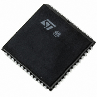
PSD834F2-70J STMicroelectronics, PSD834F2-70J Datasheet - Page 16

PSD834F2-70J
Manufacturer Part Number
PSD834F2-70J
Description
IC FLASH 2MBIT 70NS 52PLCC
Manufacturer
STMicroelectronics
Datasheet
1.PSD813F2VA-20JI.pdf
(109 pages)
Specifications of PSD834F2-70J
Format - Memory
FLASH
Memory Type
FLASH
Memory Size
2M (256K x 8)
Speed
70ns
Interface
Parallel
Voltage - Supply
4.5 V ~ 5.5 V
Operating Temperature
0°C ~ 70°C
Package / Case
52-PLCC
Lead Free Status / RoHS Status
Lead free / RoHS Compliant
Other names
497-2004-5
Available stocks
Company
Part Number
Manufacturer
Quantity
Price
Company:
Part Number:
PSD834F2-70J
Manufacturer:
WSI
Quantity:
409
Company:
Part Number:
PSD834F2-70J
Manufacturer:
STMicroelectronics
Quantity:
10 000
PSD813F2V, PSD854F2V
JTAG Port
In-System Programming (ISP) can be performed
through the JTAG signals on Port C. This serial in-
terface allows complete programming of the entire
PSD device. A blank device can be completely
programmed. The JTAG signals (TMS, TCK,
TSTAT, TERR, TDI, TDO) can be multiplexed with
other functions on Port C. Table
JTAG pin assignments.
In-System Programming (ISP)
Using the JTAG signals on Port C, the entire PSD
device can be programmed or erased without the
use of the MCU. The primary Flash memory can
also be programmed in-system by the MCU exe-
cuting the programming algorithms out of the sec-
ondary memory, or SRAM. The secondary
memory can be programmed the same way by ex-
ecuting out of the primary Flash memory. The PLD
or other PSD Configuration blocks can be pro-
grammed through the JTAG port or a device pro-
grammer. Table
methods can program different functional blocks
of the PSD.
Power Management Unit (PMU)
The Power Management Unit (PMU) gives the
user control of the power consumption on selected
functional blocks based on system requirements.
The PMU includes an Automatic Power-down
(APD) Unit that turns off device functions during
Table 5. Methods of Programming Different Functional Blocks of the PSD
16/109
Primary Flash Memory
Secondary Flash Memory
PLD Array (DPLD and CPLD)
PSD Configuration
Functional Block
5
indicates which programming
4
indicates the
Doc ID 10552 Rev 3
Yes
Yes
Yes
Yes
JTAG Programming
MCU inactivity. The APD Unit has a Power-down
mode that helps reduce power consumption.
The PSD also has some bits that are configured at
run-time by the MCU to reduce power consump-
tion of the CPLD. The Turbo Bit in PMMR0 can be
reset to '0' and the CPLD latches its outputs and
goes to sleep until the next transition on its inputs.
Additionally, bits in PMMR2 can be set by the
MCU to block signals from entering the CPLD to
reduce power consumption. Please see the sec-
tion entitled
more details.
Table 4. JTAG SIgnals on Port C
PC0
PC1
PC3
PC4
PC5
PC6
Port C Pins
Yes
Yes
Yes
Yes
Device Programmer
POWER MANAGEMENT, page 62
TMS
TCK
TSTAT
TERR
TDI
TDO
JTAG Signal
Yes
Yes
No
No
IAP
for


