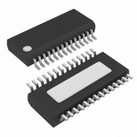
MAX3140EEI+T Maxim Integrated Products, MAX3140EEI+T Datasheet - Page 19

MAX3140EEI+T
Manufacturer Part Number
MAX3140EEI+T
Description
IC UART W/RS485 28-QSOP
Manufacturer
Maxim Integrated Products
Datasheet
1.MAX3140CEIT.pdf
(36 pages)
Specifications of MAX3140EEI+T
Features
Transceiver
Fifo's
8 Byte
Protocol
RS232, RS485
Voltage - Supply
4.75 V ~ 5.25 V
With Irda Encoder/decoder
Yes
With False Start Bit Detection
Yes
With Cmos
Yes
Mounting Type
Surface Mount
Package / Case
28-QSOP
Lead Free Status / RoHS Status
Lead free / RoHS Compliant
Configure the UART by writing a 16-bit word to the
WRITE CONFIGURATION register, which programs the
baud rate, data-word length, parity enable, and enable
of the 8-word receive FIFO. Set bits 15 and 14 of the
DIN configuration word to 1 to enable the WRITE CON-
FIGURATION mode. Bits 13–0 of the DIN configuration
word set the configuration of the UART. Table 2 shows
the bit assignment for the WRITE CONFIGURATION
register. The WRITE CONFIGURATION register allows
selection between normal UART timing and IrDA timing,
shutdown control, and contains four interrupt mask bits.
Notes:
bit 15, 14: DIN
1, 1 = Write Configuration
bit 13: DIN
FEN = 0, FIFO is enabled
FEN= 1, FIFO is disabled
bit 12: DIN
SHDNi = 1, Enter software shutdown
SHDNi = 0, Exit software shutdown
bit 11: DIN
TM = 1, Transmit-buffer-empty interrupt is enabled.
TM = 0, Transmit-buffer-empty interrupt is disabled.
bit 10: DIN
RM = 1, Data available in the receive register or FIFO interrupt
is enabled.
RM = 0, Data available in the receive register or FIFO interrupt
is disabled.
bit 9: DIN
PM = 1, Parity-bit-received interrupt is enabled.
PM = 0, Parity-bit-received interrupt is disabled.
bit 8: DIN
RAM = 1, Receiver-activity (shutdown mode)/Framing-error
(normal operation) interrupt is enabled.
RAM = 0, Receiver-activity (shutdown mode)/Framing-error
(normal operation) interrupt is disabled.
Table 2. WRITE CONFIGURATION Register Bit Assignment (D15, D14 = 1, 1)
SPI/MICROWIRE-Compatible UART with Integrated
DOUT
DIN
BIT
15
R
1
14
1
T
______________________________________________________________________________________
True Fail-Safe RS-485/RS-422 Transceivers
WRITE CONFIGURATION Register
FEN
13
0
SHDNi
12
0
(D15, D14 = 1, 1)
TM
11
0
RM
10
0
PM
9
0
RAM
8
0
Setting the WRITE CONFIGURATION register clears the
receive FIFO and the R, T, RA/FE, D0r–D7r, D0t–D7t,
Pr, and Pt registers. Bits RTS and CTS remain
unchanged. The new configuration is valid on CS’s ris-
ing edge if the transmit buffer is empty (T = 1) and
transmission is over. If the latest transmission has not
been completed (T = 0), the registers are updated
when the transmission is over.
The WRITE CONFIGURATION register bits (FEN,
SHDNi, IR, ST, PE, L, B3–B0) take effect after the cur-
rent transmission is over. The mask bits (TM, RM, PM,
RAM) take effect immediately after SCLK’s 16th rising
edge.
bit 7: DIN
IR = 1, IrDA mode is enabled.
IR = 0, IrDA mode is disabled.
bit 6: DIN
ST = 1, Transmit two stop bits
ST = 0, Transmit one stop bit
bit 5: DIN
PE = 1, Parity is enabled for both transmit (state of Pt) and
receive.
PE = 0, Parity is disabled for both transmit and receive.
bit 4: DIN
L = 1, 7-bit words (8-bit words if PE = 1)
L = 0, 8-bit words (9-bit words if PE = 1)
bit 3–0: DIN
B3–B0 = XXXX Baud-Rate Divisor select bits. See Table 6.
bit 15: DOUT
R = 1, Data is available to be read from the receive.
register or FIFO.
R = 0, Receive register and FIFO are empty.
bit 14: DOUT
T = 1, Transmit buffer is empty.
T = 0, Transmit buffer is full.
bit 13–0: DOUT
Zeros
IR
7
0
ST
6
0
PE
5
0
4
L
0
B3
3
0
B2
2
0
B1
1
0
B0
0
0
19


