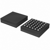
SC16C852VIET,157 NXP Semiconductors, SC16C852VIET,157 Datasheet - Page 30

SC16C852VIET,157
Manufacturer Part Number
SC16C852VIET,157
Description
IC UART DUAL W/FIFO 36TFBGA
Manufacturer
NXP Semiconductors
Datasheet
1.SC16C852VIBS557.pdf
(55 pages)
Specifications of SC16C852VIET,157
Features
Programmable
Number Of Channels
2, DUART
Fifo's
128 Byte
Protocol
RS485
Voltage - Supply
1.8V
With Auto Flow Control
Yes
With Irda Encoder/decoder
Yes
With False Start Bit Detection
Yes
With Modem Control
Yes
With Cmos
Yes
Mounting Type
Surface Mount
Package / Case
36-TFBGA
Lead Free Status / RoHS Status
Lead free / RoHS Compliant
Other names
568-4019
935282518157
SC16C852VIET
SC16C852VIET
935282518157
SC16C852VIET
SC16C852VIET
Available stocks
Company
Part Number
Manufacturer
Quantity
Price
Company:
Part Number:
SC16C852VIET,157
Manufacturer:
NXP Semiconductors
Quantity:
10 000
NXP Semiconductors
SC16C852V
Product data sheet
7.7 Line Status Register (LSR)
This register provides the status of data transfers between the SC16C852V and the CPU.
Table 22.
Bit
7
6
5
4
3
2
1
0
Symbol
LSR[7]
LSR[6]
LSR[5]
LSR[4]
LSR[3]
LSR[2]
LSR[1]
LSR[0]
Line Status Register bits description
Dual UART with 128-byte FIFOs, IrDA, and XScale VLIO bus interface
All information provided in this document is subject to legal disclaimers.
Description
FIFO data error.
THR and TSR empty. This bit is the Transmit Empty indicator. This bit is set to a
logic 1 whenever the transmit holding register and the transmit shift register are
both empty. It is reset to logic 0 whenever either the THR or TSR contains a
data character. In the FIFO mode, this bit is set to logic 1 whenever the transmit
FIFO and transmit shift register are both empty.
THR empty. This bit is the Transmit Holding Register Empty indicator. This bit
indicates that the UART is ready to accept a new character for transmission. In
addition, this bit causes the UART to issue an interrupt to CPU when the THR
interrupt enable is set. The THR bit is set to a logic 1 when a character is
transferred from the transmit holding register into the transmitter shift register.
The bit is reset to a logic 0 concurrently with the loading of the transmitter
holding register by the CPU. In the FIFO mode, this bit is set when the transmit
FIFO is empty; it is cleared when at least 1 byte is written to the transmit FIFO.
Break interrupt.
Framing error.
Parity error.
Overrun error.
Receive data ready.
logic 0 = no error (normal default condition)
logic 1 = at least one parity error, framing error or break indication is in the
current FIFO data. This bit is cleared when there are no remaining error flags
associated with the remaining data in the FIFO.
logic 0 = no break condition (normal default condition)
logic 1 = the receiver received a break signal (RX was a logic 0 for one
character frame time). In the FIFO mode, only one break character is loaded
into the FIFO.
logic 0 = no framing error (normal default condition)
logic 1 = framing error. The receive character did not have a valid stop bit(s).
In the FIFO mode, this error is associated with the character at the top of the
FIFO.
logic 0 = no parity error (normal default condition
logic 1 = parity error. The receive character does not have correct parity
information and is suspect. In the FIFO mode, this error is associated with the
character at the top of the FIFO.
logic 0 = no overrun error (normal default condition)
logic 1 = overrun error. A data overrun error occurred in the Receive Shift
Register. This happens when additional data arrives while the FIFO is full. In
this case, the previous data in the shift register is overwritten. Note that under
this condition, the data byte in the Receive Shift Register is not transferred
into the FIFO, therefore the data in the FIFO is not corrupted by the error.
logic 0 = no data in Receive Holding Register or FIFO (normal default
condition)
logic 1 = data has been received and is saved in the Receive Holding
Register or FIFO
Rev. 5 — 21 January 2011
SC16C852V
© NXP B.V. 2011. All rights reserved.
30 of 55


