SC16IS740IPW,112 NXP Semiconductors, SC16IS740IPW,112 Datasheet - Page 24
SC16IS740IPW,112
Manufacturer Part Number
SC16IS740IPW,112
Description
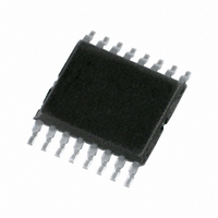
IC UART SINGLE W/FIFO 16-TSSOP
Manufacturer
NXP Semiconductors
Type
UART with 64-byte FIFOs and IrDA encoder/decoderr
Datasheet
1.SC16IS740IPW112.pdf
(62 pages)
Specifications of SC16IS740IPW,112
Number Of Channels
1, UART
Package / Case
16-TSSOP (0.173", 4.40mm Width)
Fifo's
64 Byte
Protocol
RS232, RS485
Voltage - Supply
2.5V, 3.3V, 5V
With Auto Flow Control
Yes
With False Start Bit Detection
Yes
With Modem Control
Yes
Mounting Type
Surface Mount
Data Rate
5 Mbps
Supply Voltage (max)
3.6 V
Supply Voltage (min)
2.3 V
Supply Current
6 mA
Maximum Operating Temperature
+ 85 C
Minimum Operating Temperature
- 40 C
Mounting Style
SMD/SMT
Operating Supply Voltage
2.5 V, 3.3 V
Lead Free Status / RoHS Status
Lead free / RoHS Compliant
For Use With
568-4000 - DEMO BOARD SPI/I2C TO DUAL UART568-3510 - DEMO BOARD SPI/I2C TO UART
Lead Free Status / Rohs Status
Lead free / RoHS Compliant
Other names
568-3648-5
935280988112
SC16IS740IPW
935280988112
SC16IS740IPW
Available stocks
Company
Part Number
Manufacturer
Quantity
Price
Company:

Part Number:
SC16IS740IPW,112
Manufacturer:
JAMICON
Quantity:
101


NXP Semiconductors
SC16IS740_750_760_6
Product data sheet
8.4 Line Control Register (LCR)
[1]
This register controls the data communication format. The word length, number of stop
bits, and parity type are selected by writing the appropriate bits to the LCR.
shows the Line Control Register bit settings.
Table 12.
Bit
7
6
5
4
3
2
1:0
FIFO reset requires at least two XTAL1 clocks, therefore, they cannot be reset without the presence of the
XTAL1 clock.
Symbol
LCR[7]
LCR[6]
LCR[5]
LCR[4]
LCR[3]
LCR[2]
LCR[1:0]
Line Control Register bits description
Single UART with I
Description
divisor latch enable
Break control bit. When enabled, the break control bit causes a break
condition to be transmitted (the TX output is forced to a logic 0 state).
This condition exists until disabled by setting LCR[6] to a logic 0.
Set parity. LCR[5] selects the forced parity format (if LCR[3] = 1).
parity type select
parity enable
Number of stop bits. Specifies the number of stop bits.
Word length bits 1, 0. These two bits specify the word length to be
transmitted or received; see
Rev. 06 — 13 May 2008
logic 0 = divisor latch disabled (normal default condition)
logic 1 = divisor latch enabled
logic 0 = no TX break condition (normal default condition).
logic 1 = forces the transmitter output (TX) to a logic 0 to alert the
communication terminal to a line break condition
logic 0 = parity is not forced (normal default condition).
LCR[5] = logic 1 and LCR[4] = logic 0: parity bit is forced to a logical 1
for the transmit and receive data.
LCR[5] = logic 1 and LCR[4] = logic 1: parity bit is forced to a logical 0
for the transmit and receive data.
logic 0 = odd parity is generated (if LCR[3] = 1)
logic 1 = even parity is generated (if LCR[3] = 1)
logic 0 = no parity (normal default condition).
logic 1 = a parity bit is generated during transmission and the receiver
checks for received parity
0 to 1 stop bit (word length = 5, 6, 7, 8)
1 to 1.5 stop bits (word length = 5)
1 = 2 stop bits (word length = 6, 7, 8)
2
C-bus/SPI interface, 64-byte FIFOs, IrDA SIR
SC16IS740/750/760
Table
15.
© NXP B.V. 2008. All rights reserved.
Table 12
24 of 62
Related parts for SC16IS740IPW,112
Image
Part Number
Description
Manufacturer
Datasheet
Request
R

Part Number:
Description:
NXP Semiconductors designed the LPC2420/2460 microcontroller around a 16-bit/32-bitARM7TDMI-S CPU core with real-time debug interfaces that include both JTAG andembedded trace
Manufacturer:
NXP Semiconductors
Datasheet:

Part Number:
Description:
NXP Semiconductors designed the LPC2458 microcontroller around a 16-bit/32-bitARM7TDMI-S CPU core with real-time debug interfaces that include both JTAG andembedded trace
Manufacturer:
NXP Semiconductors
Datasheet:
Part Number:
Description:
NXP Semiconductors designed the LPC2468 microcontroller around a 16-bit/32-bitARM7TDMI-S CPU core with real-time debug interfaces that include both JTAG andembedded trace
Manufacturer:
NXP Semiconductors
Datasheet:
Part Number:
Description:
NXP Semiconductors designed the LPC2470 microcontroller, powered by theARM7TDMI-S core, to be a highly integrated microcontroller for a wide range ofapplications that require advanced communications and high quality graphic displays
Manufacturer:
NXP Semiconductors
Datasheet:
Part Number:
Description:
NXP Semiconductors designed the LPC2478 microcontroller, powered by theARM7TDMI-S core, to be a highly integrated microcontroller for a wide range ofapplications that require advanced communications and high quality graphic displays
Manufacturer:
NXP Semiconductors
Datasheet:
Part Number:
Description:
The Philips Semiconductors XA (eXtended Architecture) family of 16-bit single-chip microcontrollers is powerful enough to easily handle the requirements of high performance embedded applications, yet inexpensive enough to compete in the market for hi
Manufacturer:
NXP Semiconductors
Datasheet:
Part Number:
Description:
The XA-S3 device is a member of Philips Semiconductors? XA(eXtended Architecture) family of high performance 16-bitsingle-chip microcontrollers
Manufacturer:
NXP Semiconductors
Datasheet:

Part Number:
Description:
The NXP BlueStreak LH75401/LH75411 family consists of two low-cost 16/32-bit System-on-Chip (SoC) devices
Manufacturer:
NXP Semiconductors
Datasheet:
Part Number:
Description:
The NXP LPC3130/3131 combine an 180 MHz ARM926EJ-S CPU core, high-speed USB2
Manufacturer:
NXP Semiconductors
Datasheet:
Part Number:
Description:
The NXP LPC3141 combine a 270 MHz ARM926EJ-S CPU core, High-speed USB 2
Manufacturer:
NXP Semiconductors
Part Number:
Description:
The NXP LPC3143 combine a 270 MHz ARM926EJ-S CPU core, High-speed USB 2
Manufacturer:
NXP Semiconductors

Part Number:
Description:
The NXP LPC3152 combines an 180 MHz ARM926EJ-S CPU core, High-speed USB 2
Manufacturer:
NXP Semiconductors
Part Number:
Description:
The NXP LPC3154 combines an 180 MHz ARM926EJ-S CPU core, High-speed USB 2
Manufacturer:
NXP Semiconductors

Part Number:
Description:
Standard level N-channel enhancement mode Field-Effect Transistor (FET) in a plastic package using NXP High-Performance Automotive (HPA) TrenchMOS technology
Manufacturer:
NXP Semiconductors
Datasheet: