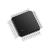
SC28L92A1B NXP Semiconductors, SC28L92A1B Datasheet - Page 49

SC28L92A1B
Manufacturer Part Number
SC28L92A1B
Description
UART Interface IC UART DUAL W/FIFO
Manufacturer
NXP Semiconductors
Type
Dual UARTr
Datasheet
1.SC28L92A1B557.pdf
(73 pages)
Specifications of SC28L92A1B
Number Of Channels
2
Data Rate
230.4 Kbps
Supply Voltage (max)
5 V
Supply Voltage (min)
3.3 V
Supply Current
25 mA
Maximum Operating Temperature
+ 85 C
Minimum Operating Temperature
- 40 C
Package / Case
PQFP-44
Description/function
Single-chip CMOS-LSI communications device
Mounting Style
SMD/SMT
Operating Supply Voltage
3.3 V, 5 V
Lead Free Status / Rohs Status
Details
Other names
SC28L92A1B,557
Available stocks
Company
Part Number
Manufacturer
Quantity
Price
Part Number:
SC28L92A1B
Manufacturer:
PHILIPS/飞利浦
Quantity:
20 000
Company:
Part Number:
SC28L92A1B,528
Manufacturer:
NXP Semiconductors
Quantity:
10 000
Company:
Part Number:
SC28L92A1B,551
Manufacturer:
NXP Semiconductors
Quantity:
10 000
Company:
Part Number:
SC28L92A1B,557
Manufacturer:
NXP Semiconductors
Quantity:
10 000
Company:
Part Number:
SC28L92A1BS,528
Manufacturer:
NXP Semiconductors
Quantity:
10 000
Company:
Part Number:
SC28L92A1BS,551
Manufacturer:
NXP Semiconductors
Quantity:
10 000
NXP Semiconductors
SC28L92_7
Product data sheet
7.4 Output port notes
7.5 The CTS, RTS, CTS enable Tx signals
The counter ready status bit (ISR[3]) is set once each cycle of the square wave. The bit is
reset by a stop counter command (read with A3 to A0 = 1111). The command however,
does not stop the C/T. The generated square wave is output on OP3 if it is programmed to
be the C/T output. In the counter mode, the value C/T loaded into CTPU and CTPL by the
CPU is counted down to 0. Counting begins upon receipt of a start counter command.
Upon reaching terminal count 0x0000, the counter ready interrupt bit (ISR[3]) is set. The
counter continues counting past the terminal count until stopped by the CPU. If OP3 is
programmed to be the output of the C/T, the output remains HIGH until terminal count is
reached, at which time it goes LOW. The output returns to the HIGH state and ISR[3] is
cleared when the counter is stopped by a stop counter command. The CPU may change
the values of CTPU and CTPL at any time, but the new count becomes effective only on
the next start counter commands. If new values have not been loaded, the previous count
values are preserved and used for the next count cycle.
In the counter mode, the current value of the upper and lower 8 bits of the counter (CTU,
CTL) may be read by the CPU. It is recommended that the counter be stopped when
reading to prevent potential problems which may occur if a carry from the lower 8 bits to
the upper 8 bits occurs between the times that both halves of the counter are read.
However, note that a subsequent start counter command will cause the counter to begin a
new count cycle using the values in CTPU and CTPL.
When the C/T clock divided by 16 is selected, the maximum divisor becomes 1,048,575.
The output ports are controlled from four places: the OPCR register, the OPR register, the
MR registers and the command register (except the SCC2681 and SCC68681). The
OPCR register controls the source of the data for the output ports OP2 to OP7. The data
source for output ports OP0 and OP1 is controlled by the MR and CR registers. When the
OPR is the source of the data for the output ports, the data at the ports is inverted from
that in the OPR register.
The content of the OPR register is controlled by the Set Output Port bits command and
the Reset Output Port bits command. These commands are at 0xE and 0xF, respectively.
When these commands are used, action takes place only at the bit locations where ones
exist. For example, a logic 1 in bit location 5 of the data word used with the Set Output
Port bits command will result in OPR5 being set to one. The OP5 would then be set to
logic 0 (V
Reset Output Ports bits command would set OPR5 to logic 0 and, hence, the pin OP5 to a
logic 1 (V
Clear To Send (CTS) is usually meant to be a signal to the transmitter meaning that it may
transmit data to the receiver. The CTS input is on pin IP0 for TxA and on IP1 for TxB. The
CTS signal is active LOW; thus, it is called CTSAN for TxA and CTSBN for TxB. RTS is
usually meant to be a signal from the receiver indicating that the receiver is ready to
receive data. It is also active LOW and is, thus, called RTSAN for RxA and RTSBN for
RxB. RTSAN is on pin OP0 and RTSBN is on OP1. A receiver’s RTS output will usually be
connected to the CTS input of the associated transmitter. Therefore, one could say that
RTS and CTS are different ends of the same wire.
SS
DD
). Similarly, a logic 1 in bit position 5 of the data word associated with the
).
Rev. 07 — 19 December 2007
3.3 V/5.0 V Dual Universal Asynchronous Receiver/Transmitter
SC28L92
© NXP B.V. 2007. All rights reserved.
49 of 73


