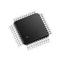
SC28L92A1B NXP Semiconductors, SC28L92A1B Datasheet - Page 4

SC28L92A1B
Manufacturer Part Number
SC28L92A1B
Description
UART Interface IC UART DUAL W/FIFO
Manufacturer
NXP Semiconductors
Type
Dual UARTr
Datasheet
1.SC28L92A1B557.pdf
(73 pages)
Specifications of SC28L92A1B
Number Of Channels
2
Data Rate
230.4 Kbps
Supply Voltage (max)
5 V
Supply Voltage (min)
3.3 V
Supply Current
25 mA
Maximum Operating Temperature
+ 85 C
Minimum Operating Temperature
- 40 C
Package / Case
PQFP-44
Description/function
Single-chip CMOS-LSI communications device
Mounting Style
SMD/SMT
Operating Supply Voltage
3.3 V, 5 V
Lead Free Status / Rohs Status
Details
Other names
SC28L92A1B,557
Available stocks
Company
Part Number
Manufacturer
Quantity
Price
Part Number:
SC28L92A1B
Manufacturer:
PHILIPS/飞利浦
Quantity:
20 000
Company:
Part Number:
SC28L92A1B,528
Manufacturer:
NXP Semiconductors
Quantity:
10 000
Company:
Part Number:
SC28L92A1B,551
Manufacturer:
NXP Semiconductors
Quantity:
10 000
Company:
Part Number:
SC28L92A1B,557
Manufacturer:
NXP Semiconductors
Quantity:
10 000
Company:
Part Number:
SC28L92A1BS,528
Manufacturer:
NXP Semiconductors
Quantity:
10 000
Company:
Part Number:
SC28L92A1BS,551
Manufacturer:
NXP Semiconductors
Quantity:
10 000
NXP Semiconductors
4. Block diagram
SC28L92_7
Product data sheet
Fig 1. Block diagram (80xxx mode)
The data pins TxD and RxD are considered idle at the logic 1 (HIGH) level when inactive, or active when at the logic 0
(LOW) level. Comments about these levels when RS232 is referenced often refer to Mark and Space levels. Mark usually
means inactive and Space means active. The voltage levels represented by the terms Mark and Space are often reversed
from those above: Mark is low voltage, and Space is high voltage.
to V
open or connect
CC
for 80xxx
D0 to D7
A0 to A3
X1/CLK
RESET
INTRN
WRN
RDN
CEN
I/M
X2
8
4
SC28L92 (80xxx mode)
R/W CONTROL
BUS BUFFER
GENERATOR
OSCILLATOR
SELECTORS
OPERATION
INTERRUPT
BAUD RATE
COUNTER/
CONTROL
ADDRESS
CONTROL
DECODE
TIMING
CLOCK
TIMER
CSRA
CSRB
XTAL
ACR
CTU
IMR
CTL
ISR
GP
Rev. 07 — 19 December 2007
3.3 V/5.0 V Dual Universal Asynchronous Receiver/Transmitter
SHIFT REGISTER
SHIFT REGISTER
TRANSMIT FIFO
DETECTORS (4)
SELECT LOGIC
OUTPUT PORT
RECEIVE FIFO
CHANGE-OF-
MRA0, 1, 2, 3
INPUT PORT
WATCHDOG
CHANNEL A
CHANNEL B
(AS ABOVE)
TRANSMIT
FUNCTION
RECEIVE
16-BYTE
16-BYTE
TIMER
STATE
OPCR
IPCR
OPR
CRA
SRA
ACR
002aad459
7
8
TxDA
RxDA
TxDB
RxDB
IP0 to IP6
OP0 to OP7
SC28L92
© NXP B.V. 2007. All rights reserved.
4 of 73


