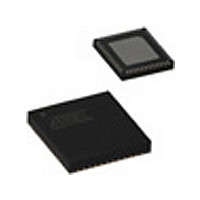
ATA5824-PLQW 80 Atmel, ATA5824-PLQW 80 Datasheet - Page 76

ATA5824-PLQW 80
Manufacturer Part Number
ATA5824-PLQW 80
Description
Manufacturer
Atmel
Datasheet
1.ATA5824-PLQW_80.pdf
(98 pages)
Specifications of ATA5824-PLQW 80
Operating Temperature (min)
-40C
Operating Temperature (max)
105C
Operating Temperature Classification
Industrial
Product Depth (mm)
7mm
Product Height (mm)
0.9mm
Product Length (mm)
7mm
Operating Supply Voltage (typ)
5V
Lead Free Status / Rohs Status
Compliant
- Current page: 76 of 98
- Download datasheet (4Mb)
17. Electrical Characteristics: General (Continued)
All parameters refer to GND and are valid for T
V
f
can be found in the specific sections of the “Electrical Characteristics”.
76
*) Type means: A = 100% tested, B = 100% correlation tested, C = Characterized on samples, D = Design parameter
Note:
RF
2.21
2.22
2.23 Blocking
VS2
No. Parameters
= 433.92 MHz (battery application) unless otherwise specified. Details about current consumption, timing and digital pin properties
= 4.4V to 5.6V, V
Useful signal to
interferer ratio
Maximum frequency
offset in ASK mode
1. Pin numbers in brackets mean they were measured with RF_IN matched to 50 according to
ATA5823/ATA5824
component values according to
page 22
VSINT
with component values according to
= 4.4V to 5.25V (car application). Typical values are given at V
Test Conditions
Peak level of useful signal to
peak level of interferer for
BER < 10
modulation scheme of
interferer.
FSK BR_Ranges 0, 1, 2
FSK BR_Range_3
ASK (P
Maximum frequency
difference of f
Receiver and transmitter in
ASK mode
P
P
According to ETSI
regulations, the sensitivity
(BER = 10
3 dB if a continuous wave
blocking signal at ± f is
signal level
(Bit rate = 20 Kbit/s,
FSK, f
Manchester code)
f
Blocking behavior see
7-3
f
Blocking behavior see
7-3
RF
RF
P
f ±0.75 MHz
f ±1.0 MHz
f ±1.5 MHz
f ±5.0 MHz
f ±10.0 MHz
f ±0.75 MHz
f ±1.0 MHz
f ±1.5 MHz
f ±5.0 MHz
f ±10.0 MHz
RF_IN
RF_IN
Block
= 315 MHz
= 433.92 MHz
to
to
DEV
Figure 7-5 on page 15
Figure 7-5 on page 15
higher than the useful
RF
+10 dBm
P
RF_IN_High
-3
< P
±19.5 kHz,
-3
with any
) is reduced by
Table 7-2 on page 12
RFIN_High
RF
amb
between
= –40°C to +105°C, V
)
Figure
Figure
Table 7-7 on page 22
Pin
(4)
(4)
(4)
(4)
(4)
(1)
(RF
IN
VS1
) and RF_OUT matched to 50 according to
SNR
SNR
Symbol
SNR
= V
f
f
P
P
OFFSET1
OFFSET2
BLOCK
BLOCK
FSK0-2
VS2
FSK3
ASK
(RF
= V
OUT
VSINT
).
Min.
VS1
–79
–85
= 2.15V to 3.6V (battery application), and
= V
VS2
= V
Typ.
10
55
57
60
66
73
54
56
59
65
67
2
4
VSINT
Figure 7-1 on page 11
= 3V and T
Max.
+79
+85
12
3
6
Figure 7-12 on
amb
4829D–RKE–06/06
Unit
dBC
dBC
kHz
dB
dB
dB
= 25°C,
Type*
with
B
B
B
B
C
C
Related parts for ATA5824-PLQW 80
Image
Part Number
Description
Manufacturer
Datasheet
Request
R

Part Number:
Description:
IC TXRX UHF ASK/FSK 48QFN
Manufacturer:
Atmel
Datasheet:

Part Number:
Description:
RF Transceiver RF Data Control Duplex Trans.
Manufacturer:
Atmel
Datasheet:

Part Number:
Description:
DEV KIT FOR AVR/AVR32
Manufacturer:
Atmel
Datasheet:

Part Number:
Description:
INTERVAL AND WIPE/WASH WIPER CONTROL IC WITH DELAY
Manufacturer:
ATMEL Corporation
Datasheet:

Part Number:
Description:
Low-Voltage Voice-Switched IC for Hands-Free Operation
Manufacturer:
ATMEL Corporation
Datasheet:

Part Number:
Description:
MONOLITHIC INTEGRATED FEATUREPHONE CIRCUIT
Manufacturer:
ATMEL Corporation
Datasheet:

Part Number:
Description:
AM-FM Receiver IC U4255BM-M
Manufacturer:
ATMEL Corporation
Datasheet:

Part Number:
Description:
Monolithic Integrated Feature Phone Circuit
Manufacturer:
ATMEL Corporation
Datasheet:

Part Number:
Description:
Multistandard Video-IF and Quasi Parallel Sound Processing
Manufacturer:
ATMEL Corporation
Datasheet:

Part Number:
Description:
High-performance EE PLD
Manufacturer:
ATMEL Corporation
Datasheet:

Part Number:
Description:
8-bit Flash Microcontroller
Manufacturer:
ATMEL Corporation
Datasheet:

Part Number:
Description:
2-Wire Serial EEPROM
Manufacturer:
ATMEL Corporation
Datasheet:


