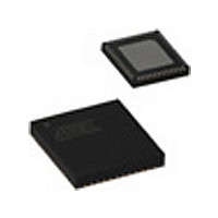
ATA5824-PLQW 80 Atmel, ATA5824-PLQW 80 Datasheet - Page 75

ATA5824-PLQW 80
Manufacturer Part Number
ATA5824-PLQW 80
Description
Manufacturer
Atmel
Datasheet
1.ATA5824-PLQW_80.pdf
(98 pages)
Specifications of ATA5824-PLQW 80
Operating Temperature (min)
-40C
Operating Temperature (max)
105C
Operating Temperature Classification
Industrial
Product Depth (mm)
7mm
Product Height (mm)
0.9mm
Product Length (mm)
7mm
Operating Supply Voltage (typ)
5V
Lead Free Status / Rohs Status
Compliant
17. Electrical Characteristics: General (Continued)
All parameters refer to GND and are valid for T
V
f
can be found in the specific sections of the “Electrical Characteristics”.
4829D–RKE–06/06
*) Type means: A = 100% tested, B = 100% correlation tested, C = Characterized on samples, D = Design parameter
Note:
RF
2.13 System bandwidth
2.14
2.15
2.16
2.17 LNA input impedance
2.18
2.19 LO spurious at LNA_IN
2.20 Image rejection
VS2
No. Parameters
= 433.92 MHz (battery application) unless otherwise specified. Details about current consumption, timing and digital pin properties
= 4.4V to 5.6V, V
System out-band
2
point with respect to f
System outband
3
point
System outband input
1 dB compression point
Allowable peak RF
input level, ASK and
FSK
nd
rd
1. Pin numbers in brackets mean they were measured with RF_IN matched to 50 according to
-order input intercept
-order input intercept
component values according to
page 22
VSINT
with component values according to
= 4.4V to 5.25V (car application). Typical values are given at V
IF
Test Conditions
This value is for
information only!
Note that for crystal and
system frequency offset
calculations, f
be used.
f
f
f
f
f
this values are for
information only, for blocking
behavior see
page 15
page 17
f
f
f
f
f
BER < 10
FSK: f
f < 1 GHz
f >1 GHz
f
f
f
Within the complete image
band
f
f
f
IF
RF
RF
RF
RF
RF
RF
RF
RF
RF
RF
RF
RF
RF
RF
RF
f
f
f
f
f
meas1
meas2
meas1
meas2
meas1
= f
= 315 MHz
= 433.92 MHz
= 868.3 MHz
= 315 MHz
= 433.92 MHz
= 868.3 MHz
= 315 MHz
= 433.92 MHz
= 868.3 MHz
= 315 MHz
= 433.92 MHz
= 868.3 MHz
= 315 MHz
= 433.92 MHz
= 868.3 MHz
DEV
meas2
= 3.6 MHz
= 10 MHz
= 1.800 MHz
= 2.026 MHz
= 1.8 MHz
to
-3
= ±19.5 kHz
, ASK: 100%
Figure 7-7 on
– f
Table 7-2 on page 12
Figure 7-3 on
amb
OFFSET
meas1
= –40°C to +105°C, V
must
Table 7-7 on page 22
Pin
(4)
(4)
(4)
(4)
(4)
(4)
(4)
(4)
(4)
(4)
(4)
(4)
(4)
(4)
(4)
(4)
(4)
(4)
4
4
4
(1)
(RF
IN
VS1
) and RF_OUT matched to 50 according to
Symbol
I1dBCP
I1dBCP
I1dBCP
P
P
Z
Z
Z
= V
SBW
IIP2
IIP3
IIP3
IIP3
IN_max
IN_max
in_LNA
in_LNA
in_LNA
VS2
(RF
= V
OUT
VSINT
).
Min.
VS1
25
25
20
= 2.15V to 3.6V (battery application), and
= V
ATA5823/ATA5824
VS2
(44 – j233)
(32 – j169)
(21 – j78)
= V
–100
Typ.
220
+50
–22
–21
–17
–31
–30
–27
+10
+10
–98
–85
30
30
25
VSINT
Figure 7-1 on page 11
= 3V and T
Max.
–10
–10
–57
–47
Figure 7-12 on
amb
dBm
dBm
dBm
dBm
dBm
dBm
dBm
dBm
dBm
dBm
dBm
dBm
dBm
dBm
Unit
kHz
dB
dB
dB
= 25°C,
Type*
with
A
C
C
C
C
C
C
C
C
C
C
C
C
C
C
C
C
C
A
A
A
75


