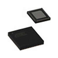
ATA5824-PLQW 80 Atmel, ATA5824-PLQW 80 Datasheet - Page 50

ATA5824-PLQW 80
Manufacturer Part Number
ATA5824-PLQW 80
Description
Manufacturer
Atmel
Datasheet
1.ATA5824-PLQW_80.pdf
(98 pages)
Specifications of ATA5824-PLQW 80
Operating Temperature (min)
-40C
Operating Temperature (max)
105C
Operating Temperature Classification
Industrial
Product Depth (mm)
7mm
Product Height (mm)
0.9mm
Product Length (mm)
7mm
Operating Supply Voltage (typ)
5V
Lead Free Status / Rohs Status
Compliant
- Current page: 50 of 98
- Download datasheet (4Mb)
13.8
50
4-wire Serial Interface
ATA5823/ATA5824
Table 13-1.
The 4-wire serial interface consists of the Chip Select (CS), the Serial Clock (SCK), the Serial
Data Input (SDI_TMDI) and the Serial Data Output (SDO_TMDO). Data is transmitted/received
bit by bit in synchronization with the serial clock.
Pin CS_POL defines the active level of the CS:
Table 13-2.
When CS is inactive and the transceiver is not in RX transparent mode, SDO_TMDO is in a
high-impedance state.
Pins SCK_POL and SCK_PHA defines the polarity and the phase of the serial clock SCK.
Figure 13-7. Serial Timing SCK_POL = 0, SCK_PHA = 0
SDO_TMDO
Command
Read TX/RX data buffer
Write TX/RX data buffer
Read control/status register
Write control register
OFF command
Delete IRQ
Not used
Not used
SDI_TMDI
CS_POL
0
1
SCK
CS
T
SCK_setup1
X
X can be either V
Command Structure
Active Level of the CS
X
Function
CS active high
CS active low
T
T
T
Setup
CS_setup
Out_enable
iL
MSB
or V
T
Hold
MSB
Bit 7
MSB
iH
0
0
0
0
1
1
1
1
T
Cycle
Bit 6
0
0
1
1
0
0
1
1
T
X
Out_delay
Bit 5
0
1
0
1
0
1
0
1
MSB-1
Bit 4
MSB-1
N4
A4
A4
X
X
X
X
X
Bit 3
X
N3
A3
A3
X
X
X
X
X
LSB
T
Bit 2
SCK_setup2
N2
A2
A2
X
X
X
X
X
X
Bit 1
4829D–RKE–06/06
N1
A1
A1
X
X
X
X
X
T
T
CS_disable
Out_disable
T
X
SCK_hold
Bit 0
LSB
N0
A0
A0
X
X
X
X
X
Related parts for ATA5824-PLQW 80
Image
Part Number
Description
Manufacturer
Datasheet
Request
R

Part Number:
Description:
IC TXRX UHF ASK/FSK 48QFN
Manufacturer:
Atmel
Datasheet:

Part Number:
Description:
RF Transceiver RF Data Control Duplex Trans.
Manufacturer:
Atmel
Datasheet:

Part Number:
Description:
DEV KIT FOR AVR/AVR32
Manufacturer:
Atmel
Datasheet:

Part Number:
Description:
INTERVAL AND WIPE/WASH WIPER CONTROL IC WITH DELAY
Manufacturer:
ATMEL Corporation
Datasheet:

Part Number:
Description:
Low-Voltage Voice-Switched IC for Hands-Free Operation
Manufacturer:
ATMEL Corporation
Datasheet:

Part Number:
Description:
MONOLITHIC INTEGRATED FEATUREPHONE CIRCUIT
Manufacturer:
ATMEL Corporation
Datasheet:

Part Number:
Description:
AM-FM Receiver IC U4255BM-M
Manufacturer:
ATMEL Corporation
Datasheet:

Part Number:
Description:
Monolithic Integrated Feature Phone Circuit
Manufacturer:
ATMEL Corporation
Datasheet:

Part Number:
Description:
Multistandard Video-IF and Quasi Parallel Sound Processing
Manufacturer:
ATMEL Corporation
Datasheet:

Part Number:
Description:
High-performance EE PLD
Manufacturer:
ATMEL Corporation
Datasheet:

Part Number:
Description:
8-bit Flash Microcontroller
Manufacturer:
ATMEL Corporation
Datasheet:

Part Number:
Description:
2-Wire Serial EEPROM
Manufacturer:
ATMEL Corporation
Datasheet:


