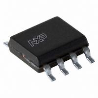
P82B96TD,118 NXP Semiconductors, P82B96TD,118 Datasheet - Page 11

P82B96TD,118
Manufacturer Part Number
P82B96TD,118
Description
IC I2C BUS BUFFER DUAL 8-SOIC
Manufacturer
NXP Semiconductors
Type
Bufferr
Datasheet
1.P82B96TD118.pdf
(32 pages)
Specifications of P82B96TD,118
Package / Case
8-SOIC (3.9mm Width)
Tx/rx Type
I²C Logic
Delay Time
5.0ns
Capacitance - Input
7pF
Voltage - Supply
2 V ~ 15 V
Current - Supply
900µA
Mounting Type
Surface Mount
Number Of Channels Per Chip
Dual
Supply Voltage (max)
15 V
Supply Voltage (min)
2 V
Maximum Operating Temperature
+ 85 C
Mounting Style
SMD/SMT
Minimum Operating Temperature
- 40 C
Logic Type
Bidirectional Bus Buffer
Lead Free Status / RoHS Status
Lead free / RoHS Compliant
For Use With
OM6285 - EVAL BOARD I2C-2002-1A568-4002 - DEMO BOARD I2C
Lead Free Status / Rohs Status
Lead free / RoHS Compliant
Other names
568-1009-2
935262295118
P82B96TD-T
935262295118
P82B96TD-T
Available stocks
Company
Part Number
Manufacturer
Quantity
Price
Company:
Part Number:
P82B96TD,118
Manufacturer:
AD
Quantity:
8 566
NXP Semiconductors
P82B96_8
Product data sheet
Figure 13
in applications that involve plug and socket connections and long cables that may become
damaged. A simple circuit is added to monitor the SDA bus, and if its LOW time exceeds
the design value, then the master bus is disconnected. P82B96 will free all its I/Os if its
supply is removed, so one option is to connect its V
say, the 74LVC family. The SDA and SCL lines could be timed and V
gate if one or other lines exceeds a design value of ‘LOW’ period as in Figure 28 of
AN255 . If the supply voltage of logic gates restricts the choice of V
low-cost discrete circuit in
capacitor will charge and the Ry input will be pulled towards V
the Ry input will set the Sy input HIGH, which in practice means simply releasing it.
In this example the SCL line is made unidirectional by tying the Rx pin to V
the buffered SCL line cannot affect the master clock line which is allowed when
clock-stretching is not required. It is simple to add an additional transistor or diode to
control the Rx input in the same way as Ry when necessary. The +V cable drive can be
any voltage up to 15 V and the bus may be run at a lower impedance by selecting pull-up
resistors for a static sink current up to 30 mA. V
connected devices. Because DDC uses relatively low speeds (< 100 kHz), the cable
length is not restricted to 20 m by the I
signalling.
Fig 13. Extending a DDC bus
V
GND
I
SDA
SCL
2
CC1
C-bus/DDC
master
shows how a master I
Sx
Sy
PC/TV receiver/decoder box
P82B96
Rev. 08 — 10 November 2009
V
CC
Figure 13
Rx
Tx
Ry
Ty
470 k
470 k
100 nF
BC
847B
4.7 k
2
C-bus can be protected against short circuits or failures
can be used. If the SDA line is held LOW, the 100 nF
+V cable drive
2
BC
847B
C-bus signalling, but it may be limited by the video
100
k
R
G
B
I
CC1
video signals
2
3 m to 20 m
C-bus/DDC
cables
CC
and V
to the output of a logic gate from,
+V cable drive
CC2
Dual bidirectional bus buffer
Rx
Ry
Tx
Ty
CC
may be chosen to suit the
monitor/flat TV
. When it exceeds 0.5V
P82B96
CC
CC
V
CC
supply then the
© NXP B.V. 2009. All rights reserved.
disabled via the
Sx
Sy
P82B96
CC
. The state of
I
slave
2
C-bus/DDC
002aab989
SCL
SDA
GND
V
CC2
11 of 32
CC


