CY8C9520A-24PVXI Cypress Semiconductor Corp, CY8C9520A-24PVXI Datasheet - Page 30
CY8C9520A-24PVXI
Manufacturer Part Number
CY8C9520A-24PVXI
Description
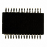
IC I/O EXPANDER I2C 20B 28SSOP
Manufacturer
Cypress Semiconductor Corp
Datasheet
1.CY8C9520A-24PVXI.pdf
(32 pages)
Specifications of CY8C9520A-24PVXI
Package / Case
28-SSOP
Interface
I²C
Number Of I /o
20
Interrupt Output
Yes
Frequency - Clock
100KHz
Voltage - Supply
3 V ~ 5.25 V
Operating Temperature
-40°C ~ 85°C
Mounting Type
Surface Mount
Includes
EEPROM, POR, PWM, WDT
Processor Series
CY8C95x0A
Core
M8C
Data Bus Width
8 bit
Maximum Clock Frequency
24 MHz
Number Of Programmable I/os
20
Operating Supply Voltage
3 V to 5.25 V
Maximum Operating Temperature
+ 85 C
Mounting Style
SMD/SMT
Development Tools By Supplier
CY3242-IOX, CY3242-IOXLite
Minimum Operating Temperature
- 40 C
On-chip Adc
8 bit
Program Memory Type
EEPROM
Program Memory Size
32 KB
Lead Free Status / RoHS Status
Lead free / RoHS Compliant
For Use With
428-2023 - KIT EVAL PSOC I2C PORT EXP428-1911 - KIT EVAL PSOC I2C PORT EXP
Lead Free Status / Rohs Status
Lead free / RoHS Compliant
Other names
428-2015-5
Available stocks
Company
Part Number
Manufacturer
Quantity
Price
Company:

Part Number:
CY8C9520A-24PVXI
Manufacturer:
LT
Quantity:
1 378
Part Number:
CY8C9520A-24PVXI
Manufacturer:
CYPRESS/赛普拉斯
Quantity:
20 000


Glossary
Document Number: 38-12036 Rev. *E
tri-state
UART
user modules
user space
V
V
watchdog timer
DD
SS
(continued)
A function whose output can adopt three states: 0, 1, and Z (high-impedance). The function does
not drive any value in the Z state and, in many respects, may be considered to be disconnected
from the rest of the circuit, allowing another output to drive the same net.
A UART or universal asynchronous receiver-transmitter translates between parallel bits of data
and serial bits.
Pre-build, pre-tested hardware/firmware peripheral functions that take care of managing and
configuring the lower level Analog and Digital PSoC Blocks. User Modules also provide high
level API (Application Programming Interface) for the peripheral function.
The bank 0 space of the register map. The registers in this bank are more likely to be modified
during normal program execution and not just during initialization. Registers in bank 1 are most
likely to be modified only during the initialization phase of the program.
A name for a power net meaning "voltage drain." The most positive power supply signal. Usually
5 V or 3.3 V.
A name for a power net meaning "voltage source." The most negative power supply signal.
A timer that must be serviced periodically. If it is not serviced, the CPU resets after a specified
period of time.
CY8C9540A, CY8C9560A
CY8C9520A
Page 30 of 32
[+] Feedback
Related parts for CY8C9520A-24PVXI
Image
Part Number
Description
Manufacturer
Datasheet
Request
R

Part Number:
Description:
CY8C9520A-24PVXIT
Manufacturer:
Cypress Semiconductor Corp
Datasheet:
Part Number:
Description:
Manufacturer:
Cypress Semiconductor Corp
Datasheet:
Part Number:
Description:
Manufacturer:
Cypress Semiconductor Corp
Datasheet:
Part Number:
Description:
Manufacturer:
Cypress Semiconductor Corp
Datasheet:
Part Number:
Description:
Manufacturer:
Cypress Semiconductor Corp
Datasheet:
Part Number:
Description:
Manufacturer:
Cypress Semiconductor Corp
Datasheet: