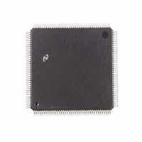
DP83905AVQB National Semiconductor, DP83905AVQB Datasheet - Page 4

DP83905AVQB
Manufacturer Part Number
DP83905AVQB
Description
IC CONTROLR AT/LAN TP IN 160PQFP
Manufacturer
National Semiconductor
Series
AT/LANTIC™r
Datasheet
1.DP83905AVQB.pdf
(80 pages)
Specifications of DP83905AVQB
Controller Type
AT, LAN Twisted-Pair Interface Controller
Voltage - Supply
4.75 V ~ 5.25 V
Current - Supply
100mA
Operating Temperature
0°C ~ 70°C
Mounting Type
Surface Mount
Package / Case
160-BFQFP
Lead Free Status / RoHS Status
Contains lead / RoHS non-compliant
Interface
-
Other names
*DP83905AVQB
Available stocks
Company
Part Number
Manufacturer
Quantity
Price
Company:
Part Number:
DP83905AVQB
Manufacturer:
Texas Instruments
Quantity:
10 000
Part Number:
DP83905AVQB
Manufacturer:
NS/国半
Quantity:
20 000
ISA BUS INTERFACE PINS
94–97
99–106
108–115
76–82
127 128
130 131
133 134
136 137
73 72
70 69
67 66
64 63
88
83
86
84
74
75
119
120
118
117
126
Pin No
2 0 Pin Description
Attachment Unit Interface TPI
Driver Types are I
SA0–SA1 9
LA17–LA23
SD0–SD15
BALE
SBHE
M16
IO16
MWR
MRD
SMRD
SMWR
IOWR
IORD
RESET
Pin Name
e
Input O
e
e
Type
Twisted Pair Interface LED
OCH
OCH
3SH
TTL
TTL
TTL
TTL
TTL
TTL
TTL
TTL
TTL
TTL
I O
Output I O
O
O
I
I
I
I
I
I
I
I
I
I
to operate correctly (See Section 6 0)
to operate correctly (See Section 6 0)
AT LANTIC Controller will use MRD and MWR in 16-bit Memory mode and will use
SMRD and SMWR in Memory mode when DWID is low (8-bit mode) SMRD and
LATCHED ADDRESS BUS Low-order 20 bits of the system’s 24 bit address bus
These lines are enabled onto the bus by the system when BALE is high and are
Iatched when BALE returns Iow These bits are used to decode accesses to the
AT LANTIC Controller’s I O map and to the boot PROM In addition they are used to
decode accesses to the AT LANTIC Controller’s memory in shared memory mode
UNLATCHED ADDRESS BUS High order 7 bits of the 24-bit system address bus
These Iines are valid on the falling edge of BALE These bits are used to decode
accesses to the AT LANTIC Controller’s memory in shared memory mode
SYSTEM DATA BUS 16-bit system data bus Used to transfer data between the
system and the AT LANTIC Controller
BUS ADDRESS LATCH ENABLE This signal indicates when the system address
lines are valid
SYSTEM BUS HIGH ENABLE This signal indicates that the system expects a
transfer on the upper byte lane
16-BIT MEMORY TRANSFER In 16-bit shared memory mode this signal indicates
that the AT LANTIC Controller has decoded an address within the 128 kbyte space
that it occupies part of
16-BIT I O TRANSFER In I O mode this signal indicates that the AT LANTIC
Controller is responding to a 16-bit I O access by driving 16-bits of data on the bus
MEMORY WRITE STROBE Strobe from system to write to AT LANTIC Controller’s
memory map This pin should be connected to allow the CHRDY fix in 16-bit I O mode
MEMORY READ STROBE Strobe from system to read from AT LANTIC Controller’s
memory map This pin should be connected to allow the CHRDY fix in 16-bit I O mode
LOW MEMORY STROBES In Memory mode these signals strobe memory transfers
in the same manner as MRD and MWR except that these signals only occur if the
access is to the lowest 1 Megabyte This partial address decode means that these
signals can be used in an 8-bit slot to properly decode an access to this area The
SMWR are also used to access the BOOT PROM
I O WRITE STROBE Strobe from system to write to the AT LANTIC Controller’s I O
map
I O READ STROBE Strobe from system to read from the AT LANTIC Controller’s
I O map
RESET This signal is output by the system to reset all devices on the bus
e
Bi-directional Output OCH
e
LED Drive MOS
4
e
Open Collector 3SH
e
CMOS Level Compatible XTAL
Description
e
TRI-STATE Output TTL
e
Crystal
e
TTL Compatible AUI
e


