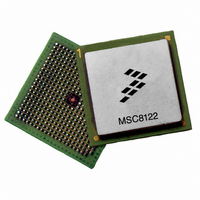
MSC8122TVT6400V Freescale Semiconductor, MSC8122TVT6400V Datasheet - Page 22

MSC8122TVT6400V
Manufacturer Part Number
MSC8122TVT6400V
Description
IC DSP QUAD 16B 400MHZ 431FCPBGA
Manufacturer
Freescale Semiconductor
Series
MSC81xx StarCorer
Type
SC140 Corer
Datasheets
1.MSC8122TVT6400V.pdf
(48 pages)
2.MSC8122TVT6400V.pdf
(2 pages)
3.MSC8122TVT6400V.pdf
(8 pages)
Specifications of MSC8122TVT6400V
Interface
DSI, Ethernet, RS-232
Clock Rate
400MHz
Non-volatile Memory
External
On-chip Ram
1.436MB
Voltage - I/o
3.30V
Voltage - Core
1.10V
Operating Temperature
0°C ~ 90°C
Mounting Type
Surface Mount
Package / Case
431-FCPBGA
For Use With
MSC8122ADSE - KIT ADVANCED DEV SYSTEM 8122
Lead Free Status / RoHS Status
Lead free / RoHS Compliant
Available stocks
Company
Part Number
Manufacturer
Quantity
Price
Company:
Part Number:
MSC8122TVT6400V
Manufacturer:
Freescale
Quantity:
1 400
Company:
Part Number:
MSC8122TVT6400V
Manufacturer:
Freescale Semiconductor
Quantity:
10 000
Electrical Characteristics
2.5.5
2.5.5.1
Generally, all MSC8122 bus and system output signals are driven from the rising edge of the reference clock (REFCLK). The
REFCLK is the
is divided by four internal ticks: T1, T2, T3, and T4. T1 always occurs at the rising edge of REFCLK (and T3 at the falling
edge), but the spacing of T2 and T4 depends on the PLL clock ratio selected, as Table 13 shows.
Figure 10 is a graphical representation of Table 13.
22
BCLK/SC140 clock
1:4, 1:6, 1:8, 1:10
System Bus Access Timing
1:3
1:5
CLKIN
Core Data Transfers
REFCLK
REFCLK
REFCLK
signal. Memory controller signals, however, trigger on four points within a REFCLK cycle. Each cycle
Figure 10. Internal Tick Spacing for Memory Controller Signals
T1
T1
T1
MSC8122 Quad Digital Signal Processor Data Sheet, Rev. 16
Table 13. Tick Spacing for Memory Controller Signals
T2
T2
T2
2/10 REFCLK
1/4 REFCLK
1/6 REFCLK
T2
T3
T3
T3
Tick Spacing (T1 Occurs at the Rising Edge of REFCLK)
T4
T4
T4
1/2 REFCLK
1/2 REFCLK
1/2 REFCLK
T3
for 1:3
for 1:5
for 1:4, 1:6, 1:8, 1:10
Freescale Semiconductor
7/10 REFCLK
3/4 REFCLK
4/6 REFCLK
T4


