ADSP-21363KSWZ-1AA Analog Devices Inc, ADSP-21363KSWZ-1AA Datasheet - Page 6
ADSP-21363KSWZ-1AA
Manufacturer Part Number
ADSP-21363KSWZ-1AA
Description
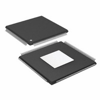
IC DSP 32BIT 333MHZ EPAD 144LQFP
Manufacturer
Analog Devices Inc
Series
SHARC®r
Type
Fixed/Floating Pointr
Datasheet
1.ADSP-21363KSWZ-1AA.pdf
(56 pages)
Specifications of ADSP-21363KSWZ-1AA
Interface
DAI, SPI
Clock Rate
333MHz
Non-volatile Memory
ROM (512 kB)
On-chip Ram
384kB
Voltage - I/o
3.30V
Voltage - Core
1.20V
Operating Temperature
0°C ~ 70°C
Mounting Type
Surface Mount
Package / Case
144-LQFP Exposed Pad, 144-eLQFP, 144-HLQFP
No. Of Bits
32 / 40
Frequency
333MHz
Supply Voltage
1.2V
Supply Voltage Range
1.14V To 1.26V
Operating Temperature Range
0°C To +70°C
Digital Ic Case Style
QFP
No. Of Pins
144
Embedded Interface Type
SPI
Rohs Compliant
Yes
Lead Free Status / RoHS Status
Lead free / RoHS Compliant
Available stocks
Company
Part Number
Manufacturer
Quantity
Price
Company:

Part Number:
ADSP-21363KSWZ-1AA
Manufacturer:
Analog Devices Inc
Quantity:
10 000


ADSP-21362/ADSP-21363/ADSP-21364/ADSP-21365/ADSP-21366
Table 3. ADSP-2136x Internal Memory Space
or test access port, will be assigned to each customer. The device
will ignore a wrong key. Emulation features and external boot
modes are only available after the correct key is scanned.
FAMILY PERIPHERAL ARCHITECTURE
The ADSP-2136x family contains a rich set of peripherals that
support a wide variety of applications, including high quality
audio, medical imaging, communications, military, test equip-
ment, 3D graphics, speech recognition, monitor control,
imaging, and other applications.
Parallel Port
The parallel port provides interfaces to SRAM and peripheral
devices. The multiplexed address and data pins (AD15–0) can
access 8-bit devices with up to 24 bits of address, or 16-bit
devices with up to 16 bits of address. In either mode, 8-bit or
16-bit, the maximum data transfer rate is 55 Mbps.
DMA transfers are used to move data to and from internal
memory. Access to the core is also facilitated through the paral-
lel port register read/write functions. The RD, WR, and ALE
(address latch enable) pins are the control pins for the
parallel port.
IOP Registers 0x0000 0000–0003 FFFF
Long Word (64 Bits)
Block 0 ROM
0x0004 0000–0x0004 7FFF
Reserved
0x0004 8000–0x0004 BFFF
Block 0 SRAM
0x0004 C000–0x0004 FFFF
Block 1 ROM
0x0005 0000–0x0005 7FFF
Reserved
0x0005 8000–0x0005 BFFF
Block 1 SRAM
0x0005 C000–0x0005 FFFF
Block 2 SRAM
0x0006 0000–0x0006 1FFF
Reserved
0x0006 2000–0x0006 FFFF
Block 3 SRAM
0x0007 0000–0x0007 1FFF
Reserved
0x0007 2000–0x0007 FFFF
Extended Precision Normal or
Instruction Word (48 Bits)
Block 0 ROM
0x0008 0000–0x0008 AAA9
Block 0 SRAM
0x0009 0000–0x0009 5554
Block 1 ROM
0x000A 0000–0x000A AAA9
Block 1 SRAM
0x000B 0000–0x000B 5554
Block 2 SRAM
0x000C 0000–0x000C 2AA9
Block 3 SRAM
0x000E 0000–0x000E 2AA9
Rev. G | Page 6 of 56 | March 2011
Normal Word (32 Bits)
Block 0 ROM
0x0008 0000–0x0008 FFFF
Reserved
0x0009 0000–0x0009 7FFF
Block 0 SRAM
0x0009 8000–0x0009 FFFF
Block 1 ROM
0x000A 0000–0x000A FFFF
Reserved
0x000B 0000–0x000B 7FFF
Block 1 SRAM
0x000B 8000–0x000B FFFF
Block 2 SRAM
0x000C 0000–0x000C 3FFF
Reserved
0x000C 4000–0x000D FFFF
Block 3 SRAM
0x000E 0000–0x000E 3FFF
Reserved
0x000E 4000–0x000F FFFF
Serial Peripheral (Compatible) Interface
The processors contain two serial peripheral interface ports
(SPIs). The SPI is an industry-standard synchronous serial link,
enabling the processor’s SPI-compatible port to communicate
with other SPI-compatible devices. The SPI consists of two data
pins, one device select pin, and one clock pin. It is a full-duplex
synchronous serial interface, supporting both master and slave
modes and can operate at a maximum baud rate of f
The SPI port can operate in a multimaster environment by
interfacing with up to four other SPI-compatible devices, either
acting as a master or slave device. The ADSP-2136x SPI-
compatible peripheral implementation also features program-
mable baud rate, clock phase, and polarities. The SPI-
compatible port uses open drain drivers to support a multimas-
ter configuration and to avoid data contention.
Pulse-Width Modulation
The entire PWM module has four groups of four PWM outputs
each. Therefore, this module generates 16 PWM outputs in
total. Each PWM group produces two pairs of PWM signals on
the four PWM outputs.
The PWM module is a flexible, programmable, PWM waveform
generator that can be programmed to generate the required
switching patterns for various applications related to motor and
engine control or audio power control. The PWM generator can
Short Word (16 Bits)
Block 0 ROM
0x0010 0000–0x0011 FFFF
Reserved
0x0012 0000–0x0012 FFFF
Block 0 SRAM
0x0013 0000–0x0013 FFFF
Block 1 ROM
0x0014 0000–0x0015 FFFF
Reserved
0x0016 0000–0x0016 FFFF
Block 1 SRAM
0x0017 0000–0x0017 FFFF
Block 2 SRAM
0x0018 0000–0x0018 7FFF
Reserved
0x0018 8000–0x001B FFFF
Block 3 SRAM
0x001C 0000–0x001C 7FFF
Reserved
0x001C 8000–0x001F FFFF
Reserved
0x0020 0000–0xFFFF FFFF
PCLK
/4.
Related parts for ADSP-21363KSWZ-1AA
Image
Part Number
Description
Manufacturer
Datasheet
Request
R

Part Number:
Description:
±1.7g Dual-Axis IMEMS Accelerometer Evaluation Board
Manufacturer:
Analog Devices Inc
Datasheet:

Part Number:
Description:
Inertial Sensor Evaluation System
Manufacturer:
Analog Devices Inc
Datasheet:
Part Number:
Description:
Manufacturer:
Analog Devices Inc
Datasheet:
Part Number:
Description:
Manufacturer:
Analog Devices Inc
Datasheet:
Part Number:
Description:
Manufacturer:
Analog Devices Inc
Datasheet:
Part Number:
Description:
Manufacturer:
Analog Devices Inc
Datasheet:
Part Number:
Description:
Manufacturer:
Analog Devices Inc
Datasheet:
Part Number:
Description:
Manufacturer:
Analog Devices Inc
Datasheet:
Part Number:
Description:
Manufacturer:
Analog Devices Inc
Datasheet:
Part Number:
Description:
Manufacturer:
Analog Devices Inc
Datasheet:
Part Number:
Description:
Manufacturer:
Analog Devices Inc
Datasheet:
Part Number:
Description:
Manufacturer:
Analog Devices Inc
Datasheet:
Part Number:
Description:
Manufacturer:
Analog Devices Inc
Datasheet: