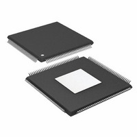
ADSP-21363KSWZ-1AA Analog Devices Inc, ADSP-21363KSWZ-1AA Datasheet - Page 26

ADSP-21363KSWZ-1AA
Manufacturer Part Number
ADSP-21363KSWZ-1AA
Description
IC DSP 32BIT 333MHZ EPAD 144LQFP
Manufacturer
Analog Devices Inc
Series
SHARC®r
Type
Fixed/Floating Pointr
Datasheet
1.ADSP-21363KSWZ-1AA.pdf
(56 pages)
Specifications of ADSP-21363KSWZ-1AA
Interface
DAI, SPI
Clock Rate
333MHz
Non-volatile Memory
ROM (512 kB)
On-chip Ram
384kB
Voltage - I/o
3.30V
Voltage - Core
1.20V
Operating Temperature
0°C ~ 70°C
Mounting Type
Surface Mount
Package / Case
144-LQFP Exposed Pad, 144-eLQFP, 144-HLQFP
No. Of Bits
32 / 40
Frequency
333MHz
Supply Voltage
1.2V
Supply Voltage Range
1.14V To 1.26V
Operating Temperature Range
0°C To +70°C
Digital Ic Case Style
QFP
No. Of Pins
144
Embedded Interface Type
SPI
Rohs Compliant
Yes
Lead Free Status / RoHS Status
Lead free / RoHS Compliant
Available stocks
Company
Part Number
Manufacturer
Quantity
Price
Company:
Part Number:
ADSP-21363KSWZ-1AA
Manufacturer:
Analog Devices Inc
Quantity:
10 000
ADSP-21362/ADSP-21363/ADSP-21364/ADSP-21365/ADSP-21366
Memory Write—Parallel Port
Use these specifications for asynchronous interfacing to memo-
ries (and memory-mapped peripherals) when the processor is
accessing external memory space.
Table 22. 8-Bit Memory Write Cycle
1
Parameter
Switching Characteristics
t
t
t
t
t
t
t
t
t
t
t
t
D = (The value set by the PPDUR Bits (5–1) in the PPCTL register) × t
H = t
F = 7 × t
On reset, ALE is an active high cycle. However, it can be configured by software to be active low.
ALEW
ADAS
ALERW
RWALE
WRH
ADAH
WW
ADWL
ADWH
DWS
DWH
DAWH
PCLK
1
1
PCLK
(if a hold cycle is specified, else H = 0)
(if FLASH_MODE is set, else F = 0). If FLASH_MODE is set, D must be 9 × t
ALE Pulse Width
AD15–0 Address Setup Before ALE Deasserted
ALE Deasserted to Write Asserted
Write Deasserted to ALE Asserted
Delay Between WR Rising Edge to Next WR Falling Edge
AD15–0 Address Hold After ALE Deasserted
WR Pulse Width
AD15–8 Address to WR Low
AD15–8 Address Hold After WR High
AD7–0 Data Setup Before WR High
AD7–0 Data Hold After WR High
AD15–8 Address to WR High
AD15
AD7
ALE
-
-
0
8
NOTE: MEMORY WRITES ALWAYS OCCUR IN GROUPS OF FOUR BETWEEN ALE CYCLES. THIS FIGURE
SHOWS ONLY TWO MEMORY WRITES TO PROVIDE THE NECESSARY TIMING INFORMATION.
t
ALEW
t
ADAS
Figure 19. Write Cycle for 8-Bit Memory Timing
ADDRESS
ADDRESS
VALID
VALID
Rev. G | Page 26 of 56 | March 2011
t
t
ADAH
ADWL
t
ALERW
VALID ADDRESS
PCLK
VALID DATA
t
t
.
DAWH
DWS
t
WW
Min
2 × t
t
2 × t
H + 0.5
F + H + t
t
D – F – 2.0
t
H
D – F + t
H
D – F + t
PCLK
PCLK
PCLK
t
WRH
K and B Grade
PCLK
PCLK
PCLK
– 2.8
– 0.5
– 2.8
.
VALID ADDRESS
PCLK
PCLK
PCLK
– 2.0
– 3.8
t
t
ADWH
DWH
VALID DATA
– 4.0
– 4.0
– 2.3
t
RWALE
Min
2 × t
t
2 × t
H + 0.5
F + H + t
t
D – F – 2.0
t
H
D – F + t
H
D – F + t
PCLK
PCLK
PCLK
PCLK
PCLK
– 2.8
– 0.5
– 3.5
Y Grade
PCLK
PCLK
PCLK
– 2.0
– 3.8
– 4.0
– 4.0
– 2.3
Unit
ns
ns
ns
ns
ns
ns
ns
ns
ns
ns
ns
ns


