AD5391BSTZ-5 Analog Devices Inc, AD5391BSTZ-5 Datasheet - Page 38
AD5391BSTZ-5
Manufacturer Part Number
AD5391BSTZ-5
Description
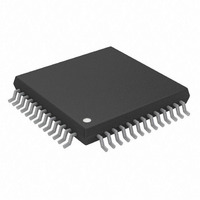
IC DAC 12BIT 16CHAN 3V 52LQFP
Manufacturer
Analog Devices Inc
Specifications of AD5391BSTZ-5
Data Interface
I²C, Serial
Design Resources
8 to 16 Channels of Programmable Voltage with Excellent Temperature Drift Performance Using AD5390/1/2 (CN0029) AD5390/91/92 Channel Monitor Function (CN0030)
Settling Time
6µs
Number Of Bits
12
Number Of Converters
16
Voltage Supply Source
Single Supply
Power Dissipation (max)
35mW
Operating Temperature
-40°C ~ 85°C
Mounting Type
Surface Mount
Package / Case
52-LQFP
Resolution (bits)
12bit
Sampling Rate
167kSPS
Input Channel Type
Serial
Supply Voltage Range - Analogue
4.5V To 5.5V
Supply Voltage Range - Digital
2.7V To 5.5V
Lead Free Status / RoHS Status
Lead free / RoHS Compliant
For Use With
EVAL-AD5391EBZ - BOARD EVALUATION FOR AD5391
Lead Free Status / RoHS Status
Lead free / RoHS Compliant, Lead free / RoHS Compliant
Available stocks
Company
Part Number
Manufacturer
Quantity
Price
Company:

Part Number:
AD5391BSTZ-5
Manufacturer:
Analog Devices Inc
Quantity:
10 000
Part Number:
AD5391BSTZ-5
Manufacturer:
ADI/亚德诺
Quantity:
20 000


AD5390/AD5391/AD5392
Digital connections have been omitted for clarity. The AD539x
contains an internal power-on reset circuit with a 10 ms brown-
out time. If the power supply ramp rate exceeds 10 ms, the user
should reset the AD539x as part of the initialization process to
ensure the calibration data is loaded correctly into the device.
AD539x MONITOR FUNCTION
The AD5390 contains a channel monitor function consisting of
a multiplexer addressed via the interface, allowing any channel
output to be routed to this pin for monitoring using an external
ADC. The channel monitor function must be enabled in the
control register before any channels are routed to the
MON_OUT pin.
Table 23 and Table 24 contain the decoding information
required to route any channel on the AD5390, AD5391, and
AD5392 to the MON_OUT pin. Selecting Channel Address 63
three-states the MON_OUT pin. The AD539x family also
contains two monitor input pins called MON_IN1 and
MON_IN2. The user can connect external signals to these
pins, which under software control can be multiplexed to
MON_OUT for monitoring purposes. Figure 42 shows a typical
monitoring circuit implemented using a 12-bit SAR ADC in a
6-lead SOT package. The external reference input is connected
to MON_IN1 to allow it to be easily monitored. The controller
output port selects the channel to be monitored, and the input
port reads the converted data from the ADC.
TOGGLE MODE FUNCTION
The toggle mode function allows an output signal to be
generated using the LDAC control signal that switches between
two DAC data registers. This function is configured using the
SFR control register, as follows. A write with REG1 = REG0 = 0,
A3–A0 = 1100 specifies a control register write. The toggle
mode function is enabled in groups of eight channels using Bits
CR3 and CR2 in the AD5390/AD5392 control register and
using Bits CR1 and CR0 in the AD5391 control register. (See
the Control Register Write section.) Figure 43 shows a block
diagram of the toggle mode implementation. Each DAC
channel on the AD539x contains an A and a B data register.
Note that the B registers can be loaded only when toggle mode
is enabled.
ADR431
AD780/
VOUT 15
VOUT 0
Figure 42. Typical Channel Monitoring Circuit
REFOUT/REFIN
MON_IN1
DAC_GND SIGNAL GND
AD5390
AV
DD
MON_OUT
SYNC
AGND
SCLK
DIN
VIN
AD7476
GND
AV
SDATA
SCLK
DD
CS
OUTPUT PORT
INPUT PORT
CONTROLLER
Rev. A | Page 38 of 44
To configure the AD539x for toggle mode of operation, the
sequence of events is as follows:
1.
2.
3.
4.
The LDAC is used to switch between the A and B registers in
determining the analog output. The first LDAC configures the
output to reflect the data in the A registers. This mode offers
significant advantages, if the user wants to generate a square
wave at the output on all channels as might be required to drive
a liquid-crystal-based, variable optical attenuator. Configuring
the AD5390, for example, the user writes to the control register
and sets CR3 = 1 and CR2 = 1, enabling the two groups of eight
for toggle mode operation. The user must then load data to all
16 A registers and B registers. Toggling the LDAC sets the out-
put values to reflect the data in the A and B registers, and the
frequency of the LDAC determines the frequency of the square
wave output. The first LDAC loads the contents of the A regis-
ters to the DAC registers. Toggle mode is disabled via the
control register; the first LDAC following the disabling of the
toggle mode updates the outputs with the data contained in the
A registers.
THERMAL MONITOR FUNCTION
The AD539x family has a temperature shutdown function to
protect the chip in case multiple outputs are shorted. The short-
circuit current of each output amplifier is typically 40 mA.
Operating the AD539x at 5 V leads to a power dissipation of
200 mW/shorted amplifier. With five channels shorted, this
leads to an extra watt of power dissipation. For the 52-lead
LQFP, the θ
The thermal monitor is enabled by the user using CR8 in the
AD5390/AD5392 control register and by CR6 in the AD5391
control register. The output amplifiers on the AD539x are
automatically powered down if the die temperature exceeds
approximately 130°C. After a thermal shutdown has occurred,
the user can re-enable the part by executing a soft power-up if
the temperature has dropped below 130°C or by turning off the
thermal monitor function via the control register.
A/B
INPUT
DATA
Enable toggle mode for the required channels via the
control register.
Load data to A registers.
Load data to B registers.
Apply LDAC .
REGISTER
INPUT
JA
is typically 44°C/W.
Figure 43. Toggle Mode Function
REGISTER
REGISTER
DATA
DATA
A
B
REGISTER
DAC
14-BIT DAC
VOUT
LDAC
CONTROL INPUT
Related parts for AD5391BSTZ-5
Image
Part Number
Description
Manufacturer
Datasheet
Request
R

Part Number:
Description:
Wideband Dual-Channel Linear Multiplier/Divider
Manufacturer:
AD [Analog Devices]
Datasheet:

Part Number:
Description:
±1.7g Dual-Axis IMEMS Accelerometer Evaluation Board
Manufacturer:
Analog Devices Inc
Datasheet:

Part Number:
Description:
Inertial Sensor Evaluation System
Manufacturer:
Analog Devices Inc
Datasheet:
Part Number:
Description:
Manufacturer:
Analog Devices Inc
Datasheet:
Part Number:
Description:
Manufacturer:
Analog Devices Inc
Datasheet:
Part Number:
Description:
Manufacturer:
Analog Devices Inc
Datasheet:
Part Number:
Description:
Manufacturer:
Analog Devices Inc
Datasheet:
Part Number:
Description:
Manufacturer:
Analog Devices Inc
Datasheet:
Part Number:
Description:
Manufacturer:
Analog Devices Inc
Datasheet:
Part Number:
Description:
Manufacturer:
Analog Devices Inc
Datasheet:
Part Number:
Description:
Manufacturer:
Analog Devices Inc
Datasheet:
Part Number:
Description:
Manufacturer:
Analog Devices Inc
Datasheet:
Part Number:
Description:
Manufacturer:
Analog Devices Inc
Datasheet: