AD5391BSTZ-5 Analog Devices Inc, AD5391BSTZ-5 Datasheet - Page 29
AD5391BSTZ-5
Manufacturer Part Number
AD5391BSTZ-5
Description
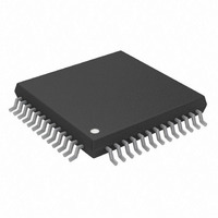
IC DAC 12BIT 16CHAN 3V 52LQFP
Manufacturer
Analog Devices Inc
Specifications of AD5391BSTZ-5
Data Interface
I²C, Serial
Design Resources
8 to 16 Channels of Programmable Voltage with Excellent Temperature Drift Performance Using AD5390/1/2 (CN0029) AD5390/91/92 Channel Monitor Function (CN0030)
Settling Time
6µs
Number Of Bits
12
Number Of Converters
16
Voltage Supply Source
Single Supply
Power Dissipation (max)
35mW
Operating Temperature
-40°C ~ 85°C
Mounting Type
Surface Mount
Package / Case
52-LQFP
Resolution (bits)
12bit
Sampling Rate
167kSPS
Input Channel Type
Serial
Supply Voltage Range - Analogue
4.5V To 5.5V
Supply Voltage Range - Digital
2.7V To 5.5V
Lead Free Status / RoHS Status
Lead free / RoHS Compliant
For Use With
EVAL-AD5391EBZ - BOARD EVALUATION FOR AD5391
Lead Free Status / RoHS Status
Lead free / RoHS Compliant, Lead free / RoHS Compliant
Available stocks
Company
Part Number
Manufacturer
Quantity
Price
Company:

Part Number:
AD5391BSTZ-5
Manufacturer:
Analog Devices Inc
Quantity:
10 000
Part Number:
AD5391BSTZ-5
Manufacturer:
ADI/亚德诺
Quantity:
20 000


3-BYTE MODE
The 3-byte mode lets the user update more than one channel in
a write sequence without having to write the device address byte
each time. The device address byte is required only once and
subsequent channel updates require the pointer byte and the
data bytes. In 3-byte mode, the user begins with an address byte
(R/ W = 0) after which the DAC acknowledges that it is
prepared to receive data by pulling SDA low. The address byte is
followed by the pointer byte; this addresses the specific channel
in the DAC to be addressed and is also acknowledged by the
DAC. Address Bits A3 to A0 address all channels on the
SCL
SDA
SCL
SDA
SDA
SDA
SCL
SCL
CONDITION
MASTER
START
BY
REG1
MSB
REG1
1
0
REG0
0
REG0
POINTER BYTE FOR CHANNEL NEXT CHANNEL
0
MSB
MOST SIGNIFICANT DATA BYTE
MOST SIGNIFICANT DATA BYTE
1
MSB
0
ADDRESS BYTE
0
0
1
A3
AD1
A2
Figure 34. The 3-Byte Mode I
AD0
A1
DATA FOR CHANNEL NEXT CHANNEL
DATA FOR CHANNEL N
LSB
R/W
LSB
A0
CONVERTER
CONVERTER
CONVERTER
CONVERTER
Rev. A | Page 29 of 44
ACK
ACK
BY
BY
ACK
ACK
BY
BY
MSB
MSB
0
MSB
2
C Write Operation
AD5390/AD5391. Address Bits A2 to A0 address all channels on
the AD5392. Address Bit A3 is a zero on the AD5392. This is
then followed by the two data bytes. REG1 and REG0 determine
the register to be updated.
If a STOP condition is not sent following the data bytes,
another channel can be updated by sending a new pointer
byte followed by the data bytes. This mode requires only three
bytes to be sent to update any channel once the device has
been addressed initially and reduces the software overhead in
updating the AD539x channels. A STOP condition at any time
exits this mode. Figure 34 shows a typical configuration.
0
POINTER BYTE FOR CHANNEL N
LEAST SIGNIFICANT DATA BYTE
LEAST SIGNIFICANT DATA BYTE
0
0
A3
A2
AD5390/AD5391/AD5392
A1
LSB
A0
CONVERTER
CONVERTER
CONVERTER
LSB
ACK
ACK
ACK
BY
BY
BY
CONDITION
MASTER
STOP
BY
Related parts for AD5391BSTZ-5
Image
Part Number
Description
Manufacturer
Datasheet
Request
R

Part Number:
Description:
Wideband Dual-Channel Linear Multiplier/Divider
Manufacturer:
AD [Analog Devices]
Datasheet:

Part Number:
Description:
±1.7g Dual-Axis IMEMS Accelerometer Evaluation Board
Manufacturer:
Analog Devices Inc
Datasheet:

Part Number:
Description:
Inertial Sensor Evaluation System
Manufacturer:
Analog Devices Inc
Datasheet:
Part Number:
Description:
Manufacturer:
Analog Devices Inc
Datasheet:
Part Number:
Description:
Manufacturer:
Analog Devices Inc
Datasheet:
Part Number:
Description:
Manufacturer:
Analog Devices Inc
Datasheet:
Part Number:
Description:
Manufacturer:
Analog Devices Inc
Datasheet:
Part Number:
Description:
Manufacturer:
Analog Devices Inc
Datasheet:
Part Number:
Description:
Manufacturer:
Analog Devices Inc
Datasheet:
Part Number:
Description:
Manufacturer:
Analog Devices Inc
Datasheet:
Part Number:
Description:
Manufacturer:
Analog Devices Inc
Datasheet:
Part Number:
Description:
Manufacturer:
Analog Devices Inc
Datasheet:
Part Number:
Description:
Manufacturer:
Analog Devices Inc
Datasheet: