AD5391BSTZ-5 Analog Devices Inc, AD5391BSTZ-5 Datasheet - Page 25
AD5391BSTZ-5
Manufacturer Part Number
AD5391BSTZ-5
Description
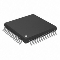
IC DAC 12BIT 16CHAN 3V 52LQFP
Manufacturer
Analog Devices Inc
Specifications of AD5391BSTZ-5
Data Interface
I²C, Serial
Design Resources
8 to 16 Channels of Programmable Voltage with Excellent Temperature Drift Performance Using AD5390/1/2 (CN0029) AD5390/91/92 Channel Monitor Function (CN0030)
Settling Time
6µs
Number Of Bits
12
Number Of Converters
16
Voltage Supply Source
Single Supply
Power Dissipation (max)
35mW
Operating Temperature
-40°C ~ 85°C
Mounting Type
Surface Mount
Package / Case
52-LQFP
Resolution (bits)
12bit
Sampling Rate
167kSPS
Input Channel Type
Serial
Supply Voltage Range - Analogue
4.5V To 5.5V
Supply Voltage Range - Digital
2.7V To 5.5V
Lead Free Status / RoHS Status
Lead free / RoHS Compliant
For Use With
EVAL-AD5391EBZ - BOARD EVALUATION FOR AD5391
Lead Free Status / RoHS Status
Lead free / RoHS Compliant, Lead free / RoHS Compliant
Available stocks
Company
Part Number
Manufacturer
Quantity
Price
Company:

Part Number:
AD5391BSTZ-5
Manufacturer:
Analog Devices Inc
Quantity:
10 000
Part Number:
AD5391BSTZ-5
Manufacturer:
ADI/亚德诺
Quantity:
20 000


INTERFACES
The AD5390/AD5391/AD5392 contain a serial interface that
can be programmed to be either DSP-, SPI-, and MICROWIRE-
compatible, or I
the interface mode.
To minimize both the power consumption of the device and
the on-chip digital noise, the interface powers up fully only
when the device is being written to—that is, on the falling
edge of SYNC .
DSP-, SPI-, AND MICROWIRE-COMPATIBLE SERIAL
INTERFACE
The serial interface can be operated with a minimum of three
wires in standalone mode or four wires in daisy-chain mode.
Daisy-chaining allows many devices to be cascaded together to
increase system channel count. The SPI/ I
Table 18. AD5390 16-Channel, 14-Bit DAC Serial Input Register Configuration
MSB
A /B
Table 19. AD5391 16-Channel, 12-Bit DAC Serial Input Register Configuration
MSB
A /B
Table 20. AD5392 8-Channel, 14-Bit DAC Serial Input Register Configuration
MSB
A /B
Table 21. Serial Input Register Configuration Bit Descriptions
Bit
A/B
R/W
A3 to A0
REG1 and REG0
DB13 to DB0
X
R/ W
R/ W
R/ W
0
0
0
2
C-compatible. The SPI/ I
0
0
0
A3
A3
0
Description
When toggle mode is enabled, this bit selects whether the data write is to the A or B register. With toggle mode
disabled, this bit should be set to zero to select the A data register.
The read or write control bit.
Used to address the input channels.
Select the register to which data is written, as outlined in Table 10.
Contain the input data-word.
Don’t care condition.
A2
A2
A2
A1
A1
A1
A0
A0
A0
REG1
REG1
REG1
2
2
C pin is used to select
C pin is tied to a
REG0
REG0
REG0
DB13
DB13
DB11
Rev. A | Page 25 of 44
DB12
DB12
DB10
DB11
DB11
DB9
Logic 1 pin to configure this mode of operation. The serial
interface control pins are described in Table 17.
Table 17. Serial Interface Control Pins
Pin
SYNC, DIN, SCLK
DCEN
SDO
Figure 2 to Figure 4 show timing diagrams for a serial write to
the AD5390/AD5391/AD5392 in both standalone and daisy-
chain mode. The 24-bit data-word format for the serial interface
is shown in Table 18 to Table 20. Descriptions of the bits follow
in Table 21.
DB10
DB8
DB10
DB7
DB9
DB9
DB6
DB8
DB8
Description
Standard 3-wire interface pins.
Selects standalone mode or daisy-chain
mode.
Data out pin for daisy-chain mode.
DB5
DB7
DB7
DB4
DB6
AD5390/AD5391/AD5392
DB6
DB3
DB5
DB5
DB2
DB4
DB4
DB1
DB3
DB3
DB0
DB2
DB2
X
DB1
DB1
LSB
X
LSB
DB0
LSB
DB0
Related parts for AD5391BSTZ-5
Image
Part Number
Description
Manufacturer
Datasheet
Request
R

Part Number:
Description:
Wideband Dual-Channel Linear Multiplier/Divider
Manufacturer:
AD [Analog Devices]
Datasheet:

Part Number:
Description:
±1.7g Dual-Axis IMEMS Accelerometer Evaluation Board
Manufacturer:
Analog Devices Inc
Datasheet:

Part Number:
Description:
Inertial Sensor Evaluation System
Manufacturer:
Analog Devices Inc
Datasheet:
Part Number:
Description:
Manufacturer:
Analog Devices Inc
Datasheet:
Part Number:
Description:
Manufacturer:
Analog Devices Inc
Datasheet:
Part Number:
Description:
Manufacturer:
Analog Devices Inc
Datasheet:
Part Number:
Description:
Manufacturer:
Analog Devices Inc
Datasheet:
Part Number:
Description:
Manufacturer:
Analog Devices Inc
Datasheet:
Part Number:
Description:
Manufacturer:
Analog Devices Inc
Datasheet:
Part Number:
Description:
Manufacturer:
Analog Devices Inc
Datasheet:
Part Number:
Description:
Manufacturer:
Analog Devices Inc
Datasheet:
Part Number:
Description:
Manufacturer:
Analog Devices Inc
Datasheet:
Part Number:
Description:
Manufacturer:
Analog Devices Inc
Datasheet: