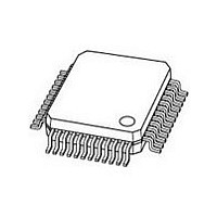
SC16C852LIB-F NXP Semiconductors, SC16C852LIB-F Datasheet - Page 29

SC16C852LIB-F
Manufacturer Part Number
SC16C852LIB-F
Description
Manufacturer
NXP Semiconductors
Datasheet
1.SC16C852LIB-F.pdf
(63 pages)
Specifications of SC16C852LIB-F
Number Of Channels
2
Transmitter And Receiver Fifo Counter
Yes
Data Rate
5Mbps
Package Type
LQFP
Mounting
Surface Mount
Pin Count
48
Operating Temperature (min)
-40C
Operating Temperature (max)
85C
Operating Temperature Classification
Industrial
Lead Free Status / Rohs Status
Compliant
NXP Semiconductors
SC16C852L_3
Product data sheet
Table 12.
[1]
[2]
Table 13.
[1]
Table 14.
[1]
Bit
3
(cont.)
2
1
0
FCR[7]
0
0
1
1
FCR[5]
0
0
1
1
For 128-byte FIFO mode, refer to
For 128-byte FIFO mode, refer to
When RXINTLVL, TXINTLVL, FLWCNTL or FLWCNTH contains any value other than 0x00, receive and
transmit trigger levels are set by RXINTLVL, TXINTLVL registers (see
When RXINTLVL, TXINTLVL, FLWCNTL or FLWCNTH contains any value other than 0x00, receive and
transmit trigger levels are set by RXINTLVL, TXINTLVL registers (see
Symbol
FCR[2]
FCR[1]
FCR[0]
FIFO Control Register bits description
RCVR trigger levels
TX FIFO trigger levels
FCR[6]
0
1
0
1
FCR[4]
0
1
0
1
Description
Transmit operation in mode ‘1’: When the SC16C852L is in FIFO mode
(FCR[0] = logic 1; FCR[3] = logic 1), the TXRDYA/TXRDYB pin will be a
logic 1 when the transmit FIFO is completely full; see
operation”. It will be a logic 0 when the trigger level has been reached.
Receive operation in mode ‘1’: When the SC16C852L is in FIFO mode
(FCR[0] = logic 1; FCR[3] = logic 1) and the trigger level has been reached,
or a Receive Time-Out has occurred, the RXRDYA/RXRDYB pin will go to a
logic 0. Once activated, it will go to a logic 1 after there are no more
characters in the FIFO.
XMIT FIFO reset.
RCVR FIFO reset.
FIFO enable.
1.8 V dual UART with 128-byte FIFOs and IrDA encoder/decoder
logic 0 = no FIFO transmit reset (normal default condition)
logic 1 = clears the contents of the transmit FIFO and resets the FIFO
counter logic. This bit will return to a logic 0 after clearing the FIFO.
logic 0 = no FIFO receive reset (normal default condition)
logic 1 = clears the contents of the receive FIFO and resets the FIFO
counter logic. This bit will return to a logic 0 after clearing the FIFO.
logic 0 = disable the transmit and receive FIFO (normal default condition)
logic 1 = enable the transmit and receive FIFO
Rev. 03 — 18 January 2008
RX FIFO trigger level (bytes) in 32-byte FIFO mode
8
16
24
28
TX FIFO trigger level (bytes) in 32-byte FIFO mode
16
8
24
30
Section
Section
7.16,
7.15,
Section
Section
…continued
7.17,
7.17,
Section
Section
7.18.
7.18.
Section 6.4 “FIFO
Section 6.4 “FIFO
SC16C852L
Section 6.10 “DMA
© NXP B.V. 2008. All rights reserved.
operation”).
operation”).
[1]
[1]
29 of 63


