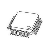
SC16C852LIB-F NXP Semiconductors, SC16C852LIB-F Datasheet - Page 21

SC16C852LIB-F
Manufacturer Part Number
SC16C852LIB-F
Description
Manufacturer
NXP Semiconductors
Datasheet
1.SC16C852LIB-F.pdf
(63 pages)
Specifications of SC16C852LIB-F
Number Of Channels
2
Transmitter And Receiver Fifo Counter
Yes
Data Rate
5Mbps
Package Type
LQFP
Mounting
Surface Mount
Pin Count
48
Operating Temperature (min)
-40C
Operating Temperature (max)
85C
Operating Temperature Classification
Industrial
Lead Free Status / Rohs Status
Compliant
NXP Semiconductors
SC16C852L_3
Product data sheet
6.12.1 Conditions to enter Sleep mode
6.12.2 Conditions to resume normal operation
6.12 Sleep mode
6.13 Low power feature
Sleep mode is an enhanced feature of the SC16C852L UART. It is enabled when EFR[4],
the enhanced functions bit, is set and when IER[4] of both channels are set.
Sleep mode is entered when:
In Sleep mode, the UART clock and baud rate clock are stopped. Since most registers are
clocked using these clocks, the power consumption is greatly reduced.
Remark: Writing to the divisor latches, DLL and DLM, to set the baud clock, must not be
done during Sleep mode. Therefore, it is advisable to disable Sleep mode using IER[4]
before writing to DLL or DLM.
SC16C852L resumes normal operation by any of the following:
If the device is awakened by one of the conditions described above, it will return to the
Sleep mode automatically after all the conditions described in
device will stay in Sleep mode until it is disabled by setting any channel’s IER bit 4 to a
logic 0.
When the SC16C852L is in Sleep mode and the host data bus (D[7:0], A[2:0], IOW, IOR,
CSA, CSB) remains in steady state, either HIGH or LOW, the Sleep mode supply current
will be in the A range as specified in
signals is toggling or floating then the sleep current will be higher.
A Low power feature is provided by the SC16C852L to prevent the switching of the host
data bus from influencing the sleep current. When the pin LOWPWR is activated (logic
HIGH), the device immediately and unconditionally goes into Low power mode. All clocks
are stopped and most host interface pins are isolated to reduce power consumption. The
device only returns to normal mode when the LOWPWR pin is de-asserted. The pin can
be left unconnected because it has an internal pull-down resistor.
•
•
•
•
•
•
•
•
Modem input pins are not toggling.
The serial data input line, RXA or RXB, is idle for 4 character time (logic HIGH) and
AFCR1[4] is logic 0. When AFCR1[4] is logic 1 the device will go to sleep regardless
of the state of the RXA/RXB pin (see
The TX FIFO and TX shift register are empty.
There are no interrupts pending.
The RX FIFO is empty.
Receives a start bit on RXA/RXB pin.
Data is loaded into transmit FIFO.
A change of state on any of the modem input pins
1.8 V dual UART with 128-byte FIFOs and IrDA encoder/decoder
Rev. 03 — 18 January 2008
Table 38 “Static
Section 7.21
characteristics”. If any of these
for the description of AFCR1 bit 4).
Section 6.12.1
SC16C852L
© NXP B.V. 2008. All rights reserved.
are met. The
21 of 63


