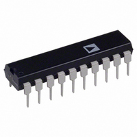
AD670JN Analog Devices Inc, AD670JN Datasheet - Page 6

AD670JN
Manufacturer Part Number
AD670JN
Description
IC ADC 8BIT SGNL COND 20-DIP
Manufacturer
Analog Devices Inc
Datasheet
1.AD670JNZ.pdf
(12 pages)
Specifications of AD670JN
Rohs Status
RoHS non-compliant
Number Of Bits
8
Sampling Rate (per Second)
10k
Data Interface
Parallel
Number Of Converters
1
Power Dissipation (max)
450mW
Voltage Supply Source
Single Supply
Operating Temperature
0°C ~ 70°C
Mounting Type
Through Hole
Package / Case
20-DIP (0.300", 7.62mm)
Available stocks
Company
Part Number
Manufacturer
Quantity
Price
Part Number:
AD670JN
Manufacturer:
ADI/亚德诺
Quantity:
20 000
Company:
Part Number:
AD670JNZ
Manufacturer:
DIODES
Quantity:
12 000
AD670
Good common-mode performance is useful in a number of situ-
ations. In bridge-type transducer applications, such performance
facilitates the recovery of differential analog signals in the pres-
ence of a dc common-mode or a noisy electrical environment.
High frequency CMRR also becomes important when the ana-
log signal is referred to a noisy, remote digital ground. In each
case, the CMRR specification of the AD670 allows the integrity
of the input signal to be preserved.
The AD670’s common-mode voltage tolerance allows great
flexibility in circuit layout. Most other A/D converters require
the establishment of one point as the analog reference point.
This is necessary in order to minimize the effects of parasitic
voltages. The AD670, however, eliminates the need to make the
analog ground reference point and A/D analog ground one and
the same. Instead, a system such as that shown in Figure 4b is
possible as a result of the AD670’s common-mode performance.
The resistors and inductors in the ground return represent un-
avoidable system parasitic impedances.
Input/Output Options
Data output coding (2s complement vs. straight binary) is
selected using Pin 12, the FORMAT pin. The selection of
input format (bipolar vs. unipolar) is controlled using Pin 11,
BPO/UPO. Prior to a write/convert, the state of FORMAT and
BPO/UPO should be available to the converter. These lines may
be tied to the data bus and may be changed with each conver-
sion if desired. The configurations are shown in Table I. Output
coding for representative signals in each of these configurations
is shown in Figure 5.
An output signal, STATUS, indicates the status of the conver-
sion. STATUS goes high at the beginning of the conversion and
returns low when the conversion cycle has been completed.
Figure 4b. AD670 Input Rejects Common-Mode
Ground Noise
Figure 4a. CMRR Over Frequency
–6–
+V
0
128 mV
255 mV
255 mV
128 mV
128 mV
+V
0
127 mV
1.127 V
255 mV
128 mV
127 mV
127 mV
–128 mV 0
Calibration
Because of its precise factory calibration, the AD670 is intended
to be operated without user trims for gun and offset; therefore,
no provisions have been made for such user trims. Figures 6a,
6b, and 6c show the transfer curves at zero and full scale for the
unipolar and bipolar modes. The code transitions are positioned
so that the desired value is centered at that code. The first LSB
transition for the unipolar mode occurs for an input of +1/2 LSB
(5 mV or 0.5 mV). Similarly, the MSB transition for the bipolar
mode is set at –1/2 LSB (–5 mV or –0.5 mV). The full scale
transition is located at the full scale value –1 1/2 LSB. These
values are 2.545 V and 254.5 mV.
Table I. AD670 Input Selection/Output Format Truth Table
IN
IN
BPO/UPO
0
1
0
1
Figure 5a. Unipolar Output Codes (Low Range)
Figure 5b. Bipolar Output Codes (Low Range)
–V
0
0
1.000 V
255 mV
127 mV
128 mV
255 mV
–V
0
0
0
255 mV
127 mV
–127 mV
IN
IN
6a. Unipolar Transfer Curve
FORMAT
0
0
1
1
DIFF
V
0
128 mV
255 mV
0
1 mV
255 mV
DIFF
V
0
127 mV
127 mV
0
1 mV
–1 mV
–128 mV
–128 mV
IN
IN
STRAIGHT BINARY
(FORMAT = 0, BPO/UPO = 0)
0000 0000
1000 0000
1111 1111
0000 0000
0000 0001
1111 1111
OFFSET BINARY 2s COMPLEMENT
(FORMAT = 0,
BPO/UPO = 1)
1000 0000
1111 1111
1111 1111
1000 0000
1000 0001
0111 1111
0000 0000
0000 0000
INPUT RANGE/
OUTPUT FORMAT
Unipolar/Straight Binary
Bipolar/Offset Binary
Unipolar/2s Complement
Bipolar/2s Complement
(FORMAT = 1,
BPO/UPO = 1)
0000 0000
0111 1111
0111 1111
0000 0000
0000 0001
1111 1111
1000 0000
1000 0000
REV. A


