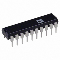
AD670JN Analog Devices Inc, AD670JN Datasheet - Page 5

AD670JN
Manufacturer Part Number
AD670JN
Description
IC ADC 8BIT SGNL COND 20-DIP
Manufacturer
Analog Devices Inc
Datasheet
1.AD670JNZ.pdf
(12 pages)
Specifications of AD670JN
Rohs Status
RoHS non-compliant
Number Of Bits
8
Sampling Rate (per Second)
10k
Data Interface
Parallel
Number Of Converters
1
Power Dissipation (max)
450mW
Voltage Supply Source
Single Supply
Operating Temperature
0°C ~ 70°C
Mounting Type
Through Hole
Package / Case
20-DIP (0.300", 7.62mm)
Available stocks
Company
Part Number
Manufacturer
Quantity
Price
Part Number:
AD670JN
Manufacturer:
ADI/亚德诺
Quantity:
20 000
Company:
Part Number:
AD670JNZ
Manufacturer:
DIODES
Quantity:
12 000
CONNECTING THE AD670
The AD670 has been designed for ease of use. All active com-
ponents required to perform a complete A/D conversion are on
board and are connected internally. In addition, all calibration
trims are performed at the factory, assuring specified accuracy
without user trims. There are, however, a number of options
and connections that should be considered to obtain maximum
flexibility from the part.
INPUT CONNECTIONS
Standard connections are shown in the figures that follow. An
input range of 0 V to 2.55 V may be configured as shown in Fig-
ure 2a. This will provide a one LSB change for each 10 mV of
input change. The input range of 0 mV to 255 mV is configured
as shown in Figure 2b. In this case, each LSB represents 1 mV
of input change. When unipolar input signals are used, Pin 11,
BPO/UPO, should be grounded. Pin 11 selects the input format
for either unipolar or bipolar signals. Figures 3a and 3b show
the input connections for bipolar signals. Pin 11 should be tied
to +V
Although the instrumentation amplifier has a differential input,
there must be a return path to ground for the bias currents. If it
is not provided, these currents will charge stray capacitances
and cause internal circuit nodes to drift uncontrollably causing
the digital output to change. Such a return path is provided in
Figures 2a and 3a (larger input ranges) since the 1k resistor leg
is tied to ground. This is not the case for Figures 2b and 3b (the
lower input ranges). When connecting the AD670 inputs to
floating sources, such as transformers and ac-coupled sources,
there must still be a dc path from each input to common. This
can be accomplished by connecting a 10 k resistor from each
input to ground.
REV. A
CC
for bipolar inputs.
NOTE: PIN 11, BPO/UPO SHOULD BE LOW WHEN
CONVERSION IS STARTED.
Figure 2. Unipolar Input Connections
2b. 0 mV to 255 mV (1 mV/LSB)
2a. 0 V to 2.55 V (10 mV/LSB)
–5–
Bipolar Operation
Through special design of the instrumentation amplifier, the
AD670 accommodates input signal excursions below ground,
even though it operates from a single 5 V supply. To the user,
this means that true bipolar input signals can be used without
the need for any additional external components. Bipolar signals
can be applied differentially across both inputs, or one of the in-
puts can be grounded and a bipolar signal applied to the other.
Common-Mode Performance
The AD670 is designed to reject dc and ac common-mode volt-
ages. In some applications it is useful to apply a differential in-
put signal V
V
listed in the specifications, which represent the maximum volt-
age V
ing proper operation. Exceeding these limits (within the range of
absolute maximum ratings), however, will not cause permanent
damage.
The excellent common-mode rejection of the AD670 is due to
the instrumentation amplifier front end, which maintains the
differential signal until it reaches the output of the comparator.
In contrast to a standard operational amplifier, the instrumenta-
tion amplifier front end provides significantly improved CMRR
over a wide frequency range (Figure 4a).
CM
. The user must observe the absolute input signal limits
IN
+ V
NOTE: PIN 11, BPO/UPO SHOULD BE HIGH WHEN
CONVERSION IS STARTED.
IN
CM
Figure 3. Bipolar Input Connections
in the presence of a dc common-mode voltage
that can be applied to either input without affect-
3b.
3a.
128 mV Range
1.28 V Range
AD670


