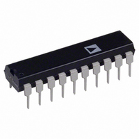
AD670JN Analog Devices Inc, AD670JN Datasheet - Page 11

AD670JN
Manufacturer Part Number
AD670JN
Description
IC ADC 8BIT SGNL COND 20-DIP
Manufacturer
Analog Devices Inc
Datasheet
1.AD670JNZ.pdf
(12 pages)
Specifications of AD670JN
Rohs Status
RoHS non-compliant
Number Of Bits
8
Sampling Rate (per Second)
10k
Data Interface
Parallel
Number Of Converters
1
Power Dissipation (max)
450mW
Voltage Supply Source
Single Supply
Operating Temperature
0°C ~ 70°C
Mounting Type
Through Hole
Package / Case
20-DIP (0.300", 7.62mm)
Available stocks
Company
Part Number
Manufacturer
Quantity
Price
Part Number:
AD670JN
Manufacturer:
ADI/亚德诺
Quantity:
20 000
Company:
Part Number:
AD670JNZ
Manufacturer:
DIODES
Quantity:
12 000
Since settling to 1/2 LSB at 8-bits of resolution requires 6.2 RC
time constants, the 500 pF hold capacitors and CD4066’s 300
on-resistance yield an acquisition time of under 1 s, assuming a
low impedance source.
This sample/hold approach makes use of the differential capa-
bilities of the AD670. Because 500 pF hold capacitors are used
on both V
the offset current of the AD670, typically 20 nA. With the
matched 500 pF capacitors, the droop rate is 40 V/ s. The in-
put will then droop only 0.4 mV (0.4 LSB) during the AD670’s
10 s conversion time. The differential approach also minimizes
pedestal error since only the difference in charge injection be-
tween the two switches results in errors at the A/D.
The fast conversion time and differential and common-mode ca-
pabilities of the AD670 permit this simple sample-hold design
to perform well with low sample-to-hold offset, droop rate of
about 40 V/ s and acquisition time under 1 s. The effective
aperture time of the AD670 is reduced by about 2 orders of
magnitude with this circuit, allowing frequencies to be con-
verted up to several kilohertz.
While no input anti-aliasing filter is shown, filtering will be nec-
essary to prevent output errors if higher frequencies are present
in the input signal. Many practical variations are possible with
this circuit, including input MUX control, for digitizing a num-
ber of ac channels.
IBM PC INTERFACE
The AD670 appears in Figure 18 interfaced to the IBM PC.
Since the device resides in I/O space, its address is decoded
from only the lower ten address lines and must be gated with
AEN (active low) to mask out internal (DMA) cycles which use
the same I/O address space. This active low signal is applied to
CS. AO, meanwhile, is reserved for the R/W input. This places
the AD670 in two adjacent addresses; one for starting the con-
version and the other for reading the result. The IOR and IOW
signals are then gated and applied to CE, while the lower two
data lines are applied to FORMAT and BPO/UPO inputs to
provide software programmable input formats and output
coding.
REV. A
Figure 17. Low Cost Sample-and-Hold Circuit for AD670
IN
+ and V
IN
– inputs, the droop rate depends only on
–11–
In BASIC, a simple OUT ADDR, WORD command initiates a
conversion. While the upper six bits of the data WORD are
meaningless, the lower two bits define the analog input format
and digital output coding according to Table IV. The data is
available ten microseconds later (which is negligible in BASIC)
and can be read using INP (ADDR + 1). The 3-line subroutine
in Figure 19, used in conjunction with the interface of Figure
18, converts an analog input within a bipolar range to an offset
binary coded digital word.
NOTE: Due to the large number of options that may be in-
stalled in the PC, the I/O bus loading should be limited to one
Schottky TTL load. Therefore, a buffer/driver should be used
when interfacing more than two AD670s to the I/O bus.
10
20
30
Data
0
1
2
3
OUT & H310,1
ANALOGIN = INP (&H311)
RETURN
Figure 18. IBM PC lnterface to AD670
Figure 19. Conversion Subroutine
Input Format
Unipolar
Bipolar
Unipolar
Bipolar
Table IV.
’INITIATE CONVERSION
’READ ANALOG INPUT
Output Coding
Straight Binary
Offset Binary
2s Complement
2s Complement
AD670


