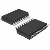
LTC1099CSW Linear Technology, LTC1099CSW Datasheet - Page 7

LTC1099CSW
Manufacturer Part Number
LTC1099CSW
Description
IC A/D CONV 8BIT HI-SPEED 20SOIC
Manufacturer
Linear Technology
Datasheet
1.LTC1099CNPBF.pdf
(16 pages)
Specifications of LTC1099CSW
Number Of Bits
8
Sampling Rate (per Second)
400k
Data Interface
Parallel
Number Of Converters
3
Power Dissipation (max)
55mW
Voltage Supply Source
Single Supply
Operating Temperature
0°C ~ 70°C
Mounting Type
Surface Mount
Package / Case
20-SOIC (0.300", 7.50mm Width)
Lead Free Status / RoHS Status
Contains lead / RoHS non-compliant
Other names
LTC1099CS
Available stocks
Company
Part Number
Manufacturer
Quantity
Price
Part Number:
LTC1099CSW
Manufacturer:
LINEAR/凌特
Quantity:
20 000
FUNCTIONAL DESCRIPTIO
Figure 5 shows the functional block diagram for the
LTC1099 2-step flash ADC. It consists of two 4-bit flash
converters, a 4-bit DAC and a differencing circuit. The
conversion process proceeds as follows:
1. At the start of the conversion, the on-board sample-
2. The held input voltage is converted by the 4-bit MS-
3. A 4-bit approximation, from the DAC output, is sub-
4. The LS-Flash ADC converts the difference between the
5. Upon the completion of the LS 4-bit flash the eight
The advantage of this approach is the reduction in the
amount of hardware required. A full flash converter re-
quires 255 comparators while this approach requires only
31. The price paid for this reduction in hardware is an
increase in conversion time. A full flash converter requires
only one comparison cycle while this approach requires
two comparison cycles, hence 2-step flash.
This architecture is further simplified in the LTC1099 by
reusing the MS-Flash hardware to do the LS-Flash. This
reduces the number of comparators from 31 to 16. This is
possible because the MS and LS conversions are done at
different times.
To take the simple block diagram of Figure 5 and reconfigure
it to reuse the MS-Flash to do the LS-Flash is conceptually
simple, but from a hardware point of view is not practical.
A new six input switched capacitor comparator is used to
and-hold switches from the sample to the hold mode.
This is a true sample-and-hold with an acquisition time
of 240ns, an aperture time of 110ns and a tracking rate
of 2.5V/ s.
Flash ADC. This generates the upper or most significant
4-bits of the 8-bit output.
tracted from the held input voltage.
held input voltage and the DAC approximation. This
generates the lower or least significant (LS) 4-bits of
the 8-bit output. The LS-Flash reference is one six-
teenth of the MS-Flash reference. This effectively mul-
tiplies the difference by 16.
output latches are updated simultaneously. At the same
time, the sample-and-hold is switched from the hold
mode to the acquire mode in preparation for the next
conversion.
U
U
U
accomplish this function in a simple, although not straight
forward, manner.
Figure 6 shows the six input switched capacitor compara-
tor. Intuitively, the comparator is easy to understand by
noting that the common connection between the two input
capacitors, C1 and C2, acts like a virtual ground. In
operational amplifier circuits, current is summed at the
virtual ground node. Input voltage is converted to current
by the input resistors. In the switched capacitor compara-
tor, input voltage is converted to charge by the input
capacitors and these charges are summed at the virtual
ground node.
A major advantage of this technique is that the switch-on
impedance has no affect on accuracy as long as sufficient
time exists to fully charge and discharge the capacitors.
During the first time period the T+ and T
closed. This forces the common node between C1 and C2
to an arbitrary bias voltage. Since the capacitors subtract
out this voltage, it may be considered, for the sake of this
discussion, to be exactly zero (i.e., virtual ground). Note
V
IN
+
Figure 5. 8-Bit 2-Step Semiflash A/D
REMAINDER
–
V
FLASH
FLASH
4-BIT
4-BIT
REF
V
MS
LS
REF
/16
4-BIT
DAC
LTC1099
Z
switches are
1099 F05
B7
B6
B5
B4
B3
B2
B1
B0
7


