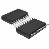
LTC1099CSW Linear Technology, LTC1099CSW Datasheet - Page 5

LTC1099CSW
Manufacturer Part Number
LTC1099CSW
Description
IC A/D CONV 8BIT HI-SPEED 20SOIC
Manufacturer
Linear Technology
Datasheet
1.LTC1099CNPBF.pdf
(16 pages)
Specifications of LTC1099CSW
Number Of Bits
8
Sampling Rate (per Second)
400k
Data Interface
Parallel
Number Of Converters
3
Power Dissipation (max)
55mW
Voltage Supply Source
Single Supply
Operating Temperature
0°C ~ 70°C
Mounting Type
Surface Mount
Package / Case
20-SOIC (0.300", 7.50mm Width)
Lead Free Status / RoHS Status
Contains lead / RoHS non-compliant
Other names
LTC1099CS
Available stocks
Company
Part Number
Manufacturer
Quantity
Price
Part Number:
LTC1099CSW
Manufacturer:
LINEAR/凌特
Quantity:
20 000
PIN
V
DB0 to DB3 (Pins 2 to 5): Data Outputs. DB0 = LSB.
WR/RDY (Pin 6): WR/RDY is an input when M0DE = V
Falling edge of WR switches internal S/H to hold then
starts conversion. WR/RDY is an open drain output (active
pull-down) when M0DE = GND. RDY goes low at start of
conversion and pull-down is turned off when conversion
is complete. Resistive pull-up is usually used in this mode.
MODE (Pin 7): WR-RD when MODE = V
M0DE = GND. No internal pull-down.
RD (Pin 8): A Low on RD with CS Low Activates Three-
State Outputs. With MODE = GND and CS low, the falling
edge of RD switches internal S/H to hold and starts
conversion.
TEST CIRCUITS
IN
U
(Pin 1): Analog Input.
FUNCTIONS
U
RD
RD
CS
CS
U
V
V
CC
CC
V
C
C
CC
L
L
1k
1k
DATA
OUT
DATA
OUT
CC
Figure 1. Three-State Test Circuit
. RD when
t
t
r
r
= 20ns, C
= 20ns, C
CC
.
t
t
1H
0H
L
L
= 10pF
= 10pF
INT (Pin 9): Output that goes low when the conversion in
process is complete and goes high after data is read.
GND (Pin 10): Ground Connection.
REF
REF
= (REF
CS (Pin 13): Chip Select. When high, data outputs are high
impedance and all inputs are ignored.
DB4 to DB7 (Pins 14 to 17): Data Outputs. DB7 = MSB.
OFL (Pin 18): Overflow Output. Goes low when V
T
V
C
CC
(Pin 19): User Adjustable Conversion Time.
–
+
(Pin 20): Positive Supply. 4.75V V
DATA OUT
DATA OUT
(Pin 11): Low Reference Potential (Analog Ground).
(Pin 12): High Reference Potential. V
+
) – (REF
RD
RD
GND
GND
GND
V
V
V
V
V
CC
CC
CC
0H
0L
–
10%
10%
).
t
t
r
r
50%
50%
90%
90%
t
1H
t
0H
90%
10%
1099 F01
LTC1099
CC
REF
= Full Scale
5.25V.
IN
> V
5
REF
.


