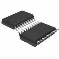
LTC1099CSW Linear Technology, LTC1099CSW Datasheet - Page 3

LTC1099CSW
Manufacturer Part Number
LTC1099CSW
Description
IC A/D CONV 8BIT HI-SPEED 20SOIC
Manufacturer
Linear Technology
Datasheet
1.LTC1099CNPBF.pdf
(16 pages)
Specifications of LTC1099CSW
Number Of Bits
8
Sampling Rate (per Second)
400k
Data Interface
Parallel
Number Of Converters
3
Power Dissipation (max)
55mW
Voltage Supply Source
Single Supply
Operating Temperature
0°C ~ 70°C
Mounting Type
Surface Mount
Package / Case
20-SOIC (0.300", 7.50mm Width)
Lead Free Status / RoHS Status
Contains lead / RoHS non-compliant
Other names
LTC1099CS
Available stocks
Company
Part Number
Manufacturer
Quantity
Price
Part Number:
LTC1099CSW
Manufacturer:
LINEAR/凌特
Quantity:
20 000
DIGITAL AND DC ELECTRICAL CHARACTERISTICS
The
SYMBOL PARAMETER
V
V
I
I
V
V
I
I
I
I
AC CHARACTERISTICS
otherwise specifications are at T
SYMBOL PARAMETER
RD Mode (Figure 2) Pin 7 = GND
t
t
t
t
t
t
t
WR/RD Mode (Figures 3 and 4) Pin 7 = V
t
t
t
t
t
t
t
t
Note 1: Absolute Maximum Ratings are those values beyond which the life
of a device may be impaired.
Note 2: All voltages are with respect to GND (Pin 10) unless otherwise
noted.
V
IH
IL
OZ
SOURCE
SINK
CC
CRD
RDY
ACC0
INTH
1H
P
ACC2
CWR
ACC0
ACC2
INTH
IHWR
1H
P
WR
IH
IL
OH
OL
CC
, t
, t
0H
= 5V, REF
0H
denotes the specifications which apply over the full operating temperature range, otherwise specifications are at T
High Level Input Voltage
Low Level Input Voltage
High Level Input Current
Low Level Input Current
High Level Output Voltage DB0-DB7, OFL, INT; V
Low Level Output Voltage DB0-DB7, OFL, INT, RDY; V
Hi-Z Output Leakage
Output Source Current
Output Sink Current
Supply Current
Conversion Time
Delay From CS to RDY
Delay From RD to Output Data Valid
Delay From RD to INT
Delay From RD to Hi-Z State on Outputs
Delay Time Between Conversions
Delay Time From RD to Output Data Valid
Conversion Time
Delay Time From WR to Output Data Valid C
Delay From RD to Output Data Valid
Delay From RD to INT
Delay From WR to INT
Delay From RD to Hi-Z State on Outputs
Delay Time Between Conversions
Minimum WR Pulse Width
+
= 5V, REF
U
–
= 0V and T
A
CONDITIONS
All Digital Inputs, V
All Digital Inputs, V
V
V
V
I
I
I
DB0-DB7, RDY; V
DB0-DB7, RDY; V
DB0-DB7, OFL, INT; V
DB0-DB7, OFL, INT, RDY; V
CS = WR = RD = V
OUT
OUT
OUT
= 25 C. V
IH
IH
IL
= 0V; All Digital Inputs
CC
= 5V; CS, RD, Mode
= 5V; WR
= 360 A
=10 A
=1.6mA
A
= T
The
MIN
CC
= 5V, REF
to T
denotes the specifications which apply over the full operating temperature range,
OUT
OUT
C
C
C
C
CC
CONDITIONS
T
C
Test Circuit Figure 1
T
C
Test Circuit Figure 1
CC
CC
MAX
A
A
L
L
L
L
L
L
L
= 25 C
= 100pF
= 100pF
= 100pF
= 25 C
= 100pF
= 100pF
= 100pF
= 100pF
CC
= 5V
= 0V
OUT
= 5.25V
= 4.75V
unless otherwise noted.
= 4.75V
+
= 0V
CC
OUT
= 5V, REF
= 4.75V
= 5V
–
= 0V and T
Note 3: Total unadjusted error includes offset, gain, linearity and hold step
errors.
Note 4: Reference input voltage range is guaranteed but is not tested.
MIN
MIN
2.2
2.2
2.0
2.4
LTC1099AI/LTC1099I
LTC1099AI/LTC1099I
A
t
t
= T
–0.0001
CWR
CRD
0.0001
0.0005
–0.1
TYP
–11
TYP
700
240
700
4.0
4.7
0.1
2.5
2.5
14
11
70
70
70
70
70
70
70
55
MIN
+ 35
+ 40
to T
MAX
MAX
MAX
0.8
0.4
2.8
2.8
5.0
–1
–3
–6
20
5.0
1
3
3
7
unless otherwise noted.
MIN
MIN
2.0
2.4
2.2
2.2
LTC1099AC/LTC1099C
LTC1099AC/LTC1099C
t
t
–0.0001
CWR
CRD
0.0001
0.0005
–0.1
TYP
–11
TYP
700
240
700
4.0
4.7
0.1
2.5
2.5
14
11
70
70
70
70
70
70
70
55
+ 35
+ 40
LTC1099
MAX
MAX
3.75
3.75
A
0.8
0.4
–3
–7
2.8
2.8
–1
15
1
3
3
9
= 25 C.
UNITS
UNITS
3
mA
mA
mA
ns
ns
ns
ns
ns
ns
ns
ns
ns
ns
ns
ns
ns
V
V
A
A
A
V
V
V
A
A
s
s
s
s


