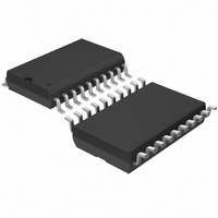
LTC1099CSW Linear Technology, LTC1099CSW Datasheet

LTC1099CSW
Specifications of LTC1099CSW
Available stocks
Related parts for LTC1099CSW
LTC1099CSW Summary of contents
Page 1
... Data outputs are latched with three-state control to allow easy interface to a processor data bus or I/O port. An overflow output (OFL) is provided to allow cascading for higher resolution. , LTC and LT are registered trademarks of Linear Technology Corporation. = 240ns) ACQ 15V 20 2.5k ...
Page 2
... REF A CC LTC1099AI/LTC1099I CONDITIONS MIN (Note – (Note 4) REF (Note 4) GND GND GND ORDER PART TOP VIEW NUMBER OFL LTC1099CSW 17 DB7 16 DB6 15 DB5 14 DB4 REF – 11 REF SW PACKAGE 20-LEAD PLASTIC SO = 150 C, = 130 C/W JA – and unless otherwise A MIN MAX LTC1099AC/LTC1099C TYP ...
Page 3
U DIGITAL AND DC ELECTRICAL CHARACTERISTICS The denotes the specifications which apply over the full operating temperature range, otherwise specifications are – 5V, REF = 5V, REF = 0V and SYMBOL PARAMETER ...
Page 4
LTC1099 W U TYPICAL PERFOR A CE CHARACTERISTICS Supply Current vs Temperature – 50 – 100 AMBIENT TEMPERATURE 1099 G01 ...
Page 5
PIN FUNCTIONS V (Pin 1): Analog Input. IN DB0 to DB3 (Pins 2 to 5): Data Outputs. DB0 = LSB. WR/RDY (Pin 6): WR/RDY is an input when M0DE = V Falling edge of WR switches internal ...
Page 6
LTC1099 DIAGRA WR/RDY INT DB0-DB7 CS WR/RDY t CWR RD INT DB0-DB7 t ACC2 Figure 3a. WR-RD Mode (Pin 7 Is HIGH and t CS (GND) RD (GND) WR/RDY INT DB0-DB7 ...
Page 7
U U FUNCTIONAL DESCRIPTIO Figure 5 shows the functional block diagram for the LTC1099 2-step flash ADC. It consists of two 4-bit flash converters, a 4-bit DAC and a differencing circuit. The conversion process proceeds as follows the ...
Page 8
LTC1099 U U FUNCTIONAL DESCRIPTIO TAP DAC 0.5 LSB 0V LS TAP T SAMPLE –1 T –2 STROBE also that variations in the bias voltage with time and temperature will also be rejected. In ...
Page 9
U DIGITAL I TERFACE The digital interface to the LTC1099 entails either control- ling the conversion timing or reading data. There are two basic modes for controlling and reading the A/D — the Write-Read(WR-RD) mode and the Read (RD) mode. ...
Page 10
LTC1099 U U ANALOG INTERFACE The inclusion of a high quality sample-and-hold (S/H) simplifies the analog interface to the LTC1099. All of the error terms normally associated with an S/H (hold step, offset, gain and droop errors) are included in ...
Page 11
U U ANALOG INTERFACE APPLICATIONS Analog Multiplier The schematic Figure 9 shows the LTC1099 configured with a DAC to form a two quadrant analog multiplier. An input waveform is applied to the LTC1099 where it is digitized at a 300kHz ...
Page 12
LTC1099 U U ANALOG INTERFACE 0 –70 32.5 Figure 11. Two Quadrant Multiplier Output Spectrum with 0V to 4.5V at 42.5kHz into LTC1099 and 2V at 5kHz into DAC 0 –70 5 11500Hz Figure 12. Two Quadrant Multiplier Output Spectrum ...
Page 13
U TYPICAL APPLICATIONS (A10, B11, H2, L6) (B1, K11, L2 TMS320C25 MSC READY STRB (B8) (C10) (4) (6) (3) (5) 1/2 74AS00 TMS320C25 Assembly Code for RD Mode Interface to LTC1099 0001 0000 0002 0032 0003 ...
Page 14
LTC1099 U TYPICAL APPLICATIONS (A10, B11, H2, L6 TMS320C25 READY MSC R/ W STRB (B8) (C10) (H11) (H10) TMS320C25 Assembly Code for WR/RD Mode Interface to LTC1099 ...
Page 15
... DIMENSION DOES NOT INCLUDE INTERLEAD FLASH. INTERLEAD FLASH SHALL NOT EXCEED 0.010" (0.254mm) PER SIDE Information furnished by Linear Technology Corporation is believed to be accurate and reliable. However, no responsibility is assumed for its use. Linear Technology Corporation makes no represen- tation that the interconnection of its circuits as described herein will not infringe on existing patent rights. ...
Page 16
... A Shutdown 5V, 60mW, 70dB SINAD 5V, 150mW, 48.5dB SINAD 5V, 80mW, 72.5dB SINAD 5V, 150mW, 81.5dB SINAD MODE REF 4 – REF 4 GND MODE REF 4 – REF 10 GND 1099 TA02 sn1099 1099fas LT/TP 1100 2K REV A • PRINTED IN USA LINEAR TECHNOLOGY CORPORATION 1989 ...


