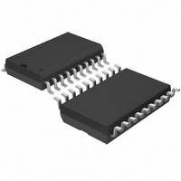
LTC1099CSW Linear Technology, LTC1099CSW Datasheet - Page 10

LTC1099CSW
Manufacturer Part Number
LTC1099CSW
Description
IC A/D CONV 8BIT HI-SPEED 20SOIC
Manufacturer
Linear Technology
Datasheet
1.LTC1099CNPBF.pdf
(16 pages)
Specifications of LTC1099CSW
Number Of Bits
8
Sampling Rate (per Second)
400k
Data Interface
Parallel
Number Of Converters
3
Power Dissipation (max)
55mW
Voltage Supply Source
Single Supply
Operating Temperature
0°C ~ 70°C
Mounting Type
Surface Mount
Package / Case
20-SOIC (0.300", 7.50mm Width)
Lead Free Status / RoHS Status
Contains lead / RoHS non-compliant
Other names
LTC1099CS
Available stocks
Company
Part Number
Manufacturer
Quantity
Price
Part Number:
LTC1099CSW
Manufacturer:
LINEAR/凌特
Quantity:
20 000
LTC1099
ANALOG INTERFACE
The inclusion of a high quality sample-and-hold (S/H)
simplifies the analog interface to the LTC1099. All of the
error terms normally associated with an S/H (hold step,
offset, gain and droop errors) are included in the error
specifications for the A/D. This makes it easy for the
designer since all the error terms need not be taken into
account individually.
S/H Timing
A falling edge on the RD or WR input switches the S/H from
acquire to hold and starts the conversion. The aperture
time is the delay from the falling edge to the actual instant
when the S/H switches to hold. It is typically 110ns.
As soon as a conversion is complete (2.5 s typ), the S/H
switches back to the sample mode. Even though the
acquisition time is only 240ns, a new conversion cannot
be started for (700ns typ) after a conversion is completed.
Analog Input
The input to the A/D looks like a 60pF capacitor in series
with 550 (Figure 8).
10
With this high input capacitance care must be taken when
driving the inputs from a source amplifier. When the input
switch closes, an instantaneous capacitive load is applied
to the amplifier output. This acts like an impulse into the
amplifier and if it has poor phase margin the resulting
ringing can cause a considerable loss of accuracy. If the
amplifier is too slow the resulting settling tail will also
cause a loss of accuracy. The amplifier should also have
low open circuit output impedance. The LT1006 is an
U
Figure 8. Equivalent Input Circuit
V
IN
U
550
60pF
TO A/D
1099 F08
excellent amplifier in this regard. It also works with a single
supply which fits nicely with the LTC1099.
Reference Inputs
Sixteen equal valued resistors are internally connected
between REF
giving a total resistance of 3.2k between the reference
terminals. When V
all ones. When V
zeros.
Although it is most common to connect REF
reference and REF
The only restrictions are REF
must be within the supply rails. As the reference voltage is
reduced the A/D will eventually lose accuracy. Accuracy is
quite good for references down to 1V.
Even though the reference drives a resistive ladder, a lot of
capacitive switching is taking place internally. For this
reason, driving the reference has the same characteristics
as driving V
The reference has the additional problem of presenting a
DC load to the driving source. This requires the DC as well
as the AC source impedance to be low.
Good Grounding
As with any precise analog system care must be taken to
follow good grounding practices when using the LTC1099.
The most noise free environment is obtained by using a
ground plane with GND (Pin 10) and REF
it. Bypass capacitors from REF
with short leads are also required to prevent spurious
switching noise from affecting the conversion accuracy.
If a ground plane is not practical, single point grounding
techniques should be used. Ground for the A/D should not
be mixed in with other noisy grounds.
IN
+
. A fast low impedance source is necessary.
and REF
IN
IN
–
equals REF
to ground, any voltages can be used.
equals REF
–
. Each resistor is nominally 200
+
–
>REF
+
, the output code will be all
(Pin 12) and V
+
, the output code will be
–
and REF
–
(Pin 11) tied to
+
CC
+
and REF
(Pin 20)
to a 5V
–


