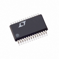
LTC2424IG Linear Technology, LTC2424IG Datasheet - Page 21

LTC2424IG
Manufacturer Part Number
LTC2424IG
Description
IC ADC 20BIT 4CH MICROPWR 28SSOP
Manufacturer
Linear Technology
Datasheet
1.LTC2424CGPBF.pdf
(36 pages)
Specifications of LTC2424IG
Number Of Bits
20
Sampling Rate (per Second)
7.5
Data Interface
MICROWIRE™, Serial, SPI™
Number Of Converters
1
Power Dissipation (max)
1mW
Voltage Supply Source
Single Supply
Operating Temperature
-40°C ~ 85°C
Mounting Type
Surface Mount
Package / Case
28-SSOP (0.200", 5.30mm Width)
Lead Free Status / RoHS Status
Contains lead / RoHS non-compliant
Available stocks
Company
Part Number
Manufacturer
Quantity
Price
Part Number:
LTC2424IG#PBF
Manufacturer:
LINEAR/凌特
Quantity:
20 000
Part Number:
LTC2424IG#TRPBF
Manufacturer:
LINEAR/凌特
Quantity:
20 000
APPLICATIONS
the 24th rising edge of SCK. On the 24th falling edge of
SCK, the device begins a new conversion. SDO goes HIGH
(EOC = 1) indicating a conversion is in progress.
At the conclusion of the data cycle, CSADC may remain
LOW and EOC monitored as an end-of-conversion inter-
rupt. Alternatively, CSADC may be driven HIGH setting
SDO to Hi-Z. As described above, CSADC may be pulled
LOW at any time in order to monitor the conversion status.
For each of these operations, CSMUX may be tied to
CSADC without affecting the selected channel.
At the conclusion of the data output cycle, the converter
enters a user transparent calibration cycle prior to actually
performing a conversion on the selected input channel.
This allows a 66ms (for 60Hz notch frequency) settling
time for the multiplexer input. Following the data output
cycle, the multiplexer input channel may be selected any
time in this 66ms window by pulling CSADC HIGH and
serial shifting data into the D
While the device is performing the internal calibration, it is
sensitive to ground current disturbances. Error currents
flowing in the ground pin may lead to offset errors. If the
SCK pin is toggling during the calibration, these ground
disturbances will occur. The solution is to either drive the
multiplexer clock input (CLK) separately from the ADC
CONVERTER
SCK/CLK
CSADC/
CSMUX
STATE
SDO
D
IN
TEST EOC
CONV
U
TEST EOC
INFORMATION
SLEEP
U
Hi-Z
Figure 14. Use of Look Ahead to Program Multiplexer After Data Output
IN
pin, see Figure 14.
BIT23
W
BIT22
DON’T CARE
BIT21
SIG
BIT20
EXR
U
BIT19 BIT18
MSB
DATA OUTPUT
BIT4
clock input (SCK), or program the multiplexer in the first
1ms following the data output cycle. The remaining 65ms
may be used to allow the input signal to settle.
Typically, CSADC remains LOW during the data output
state. However, the data output state may be aborted by
pulling CSADC HIGH anytime between the first rising edge
and the 24th falling edge of SCK, see Figure 15. On the
rising edge of CSADC, the device aborts the data output
state and immediately initiates a new conversion. This is
useful for systems not requiring all 24 bits of output data,
aborting an invalid conversion cycle or synchronizing the
start of a conversion.
Internal Serial Clock
This timing mode uses an internal serial clock to shift out
the conversion result and program the multiplexer, see
Figure 16. A CS signal directly drives the CSADC input,
while the inverse of CS drives the CSMUX input. The CS
signal is used to monitor and control the state of the
conversion cycles as well as enable the channel selection.
The multiplexer is programmed during the data output
state. The internal serial clock (SCK) generated by the ADC
is applied to the multiplexer clock input (CLK).
LSB
BIT0
EN
INTERNAL CALIBRATION
D2
66ms CALIBRATION
133ms CONVERSION CYCLE (OUTPUT RATE = 7.5Hz)
D1
LTC2424/LTC2428
D0
DON’T CARE
CONVERSION ON SELECTED CHANNEL
66ms CONVERT
21
24248 F14


