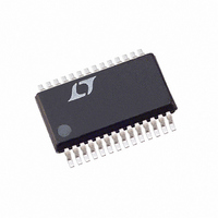
LTC2424IG Linear Technology, LTC2424IG Datasheet - Page 12

LTC2424IG
Manufacturer Part Number
LTC2424IG
Description
IC ADC 20BIT 4CH MICROPWR 28SSOP
Manufacturer
Linear Technology
Datasheet
1.LTC2424CGPBF.pdf
(36 pages)
Specifications of LTC2424IG
Number Of Bits
20
Sampling Rate (per Second)
7.5
Data Interface
MICROWIRE™, Serial, SPI™
Number Of Converters
1
Power Dissipation (max)
1mW
Voltage Supply Source
Single Supply
Operating Temperature
-40°C ~ 85°C
Mounting Type
Surface Mount
Package / Case
28-SSOP (0.200", 5.30mm Width)
Lead Free Status / RoHS Status
Contains lead / RoHS non-compliant
Available stocks
Company
Part Number
Manufacturer
Quantity
Price
Part Number:
LTC2424IG#PBF
Manufacturer:
LINEAR/凌特
Quantity:
20 000
Part Number:
LTC2424IG#TRPBF
Manufacturer:
LINEAR/凌特
Quantity:
20 000
APPLICATIONS
LTC2424/LTC2428
Ease of Use
The LTC2424/LTC2428 data output has no latency, filter
settling or redundant data associated with the conversion
cycle. There is a one-to-one correspondence between the
conversion and the output data. Therefore, multiplexing
an analog input voltage is easy.
The LTC2424/LTC2428 perform offset and full-scale cali-
brations every conversion cycle. This calibration is trans-
parent to the user and has no effect on the cyclic operation
described above. The advantage of continuous calibration
is extreme stability of offset and full-scale readings with
respect to time, supply voltage change and temperature
drift.
Power-Up Sequence
The LTC2424/LTC2428 automatically enter an internal
reset state when the power supply voltage V
below approximately 2.2V. When the V
above this critical threshold, the converter creates an
internal power-on-reset (POR) signal with duration of
approximately 0.5ms. The POR signal clears all internal
registers within the ADC and initiates a conversion. At
power-up, the multiplexer channel is disabled and should
be programmed once the device enters the sleep state.
The results of the first conversion following a POR are not
valid since a multiplexer channel was disabled.
Reference Voltage Range
The LTC2424/LTC2428 can accept a reference voltage
(V
output noise is determined by the thermal noise of the
front-end circuits, and as such, its value in microvolts is
nearly constant with reference voltage. A decrease in
reference voltage will not significantly improve the
converter’s effective resolution. On the other hand, a
reduced reference voltage will improve the overall con-
verter INL performance. The recommended range for the
LTC2424/LTC2428 voltage reference is 100mV to V
Input Voltage Range
The converter is able to accommodate system level offset
and gain errors as well as system level overrange
situations due to its extended input range, see Figure 2.
12
REF
= FS
SET
– ZS
U
SET
) from 0V to V
INFORMATION
U
W
CC
CC
. The converter
voltage rises
U
CC
drops
CC
.
The LTC2424/LTC2428 converts input signals within the
extended input range of – 0.125 • V
(V
For large values of V
range of – 0.3V to (V
ESD protection devices begin to turn on and the errors due
to the input leakage current increase rapidly.
Input signals applied to V
– 300mV and above V
current, a resistor of up to 5k may be added in series with
any channel input pin (CH0 to CH7) without affecting the
performance of the device. In the physical layout, it is im-
portant to maintain the parasitic capacitance of the connec-
tion between this series resistance and the channel input
pin as low as possible; therefore, the resistor should be
located as close as practical to the channel input pin. The
effect of the series resistance on the converter accuracy can
be evaluated from the curves presented in the Analog In-
put/Reference Current section. In addition, a series resis-
tor will introduce a temperature dependent offset error due
to the input leakage current. A 1nA input leakage current
will develop a 1ppm offset error on a 5k resistor if V
5V. This error has a very strong temperature dependency.
Output Data Format
The LTC2424/LTC2428 serial output data stream is 24 bits
long. The first 4 bits represent status information indicat-
ing the sign, input range and conversion state. The next 20
bits are the conversion result, MSB first.
ZS
FS
REF
SET
SET
+ 0.12V
– 0.12V
V
= FS
CC
+ 0.3V
ZS
–0.3V
FS
Figure 2. LTC2424/LTC2428 Input Range
SET
REF
SET
SET
REF
– ZS
NORMAL
RANGE
INPUT
SET
CC
REF
CC
V
+ 0.3V). Beyond this range the input
).
REF
by 300mV. In order to limit any fault
this range is limited to a voltage
= FS
IN
EXTENDED
may extend below ground by
RANGE
SET
INPUT
– ZS
SET
ABSOLUTE
MAXIMUM
REF
RANGE
INPUT
24248 F02
to 1.125 • V
REF
REF
=


