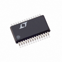
LTC2424IG Linear Technology, LTC2424IG Datasheet - Page 16

LTC2424IG
Manufacturer Part Number
LTC2424IG
Description
IC ADC 20BIT 4CH MICROPWR 28SSOP
Manufacturer
Linear Technology
Datasheet
1.LTC2424CGPBF.pdf
(36 pages)
Specifications of LTC2424IG
Number Of Bits
20
Sampling Rate (per Second)
7.5
Data Interface
MICROWIRE™, Serial, SPI™
Number Of Converters
1
Power Dissipation (max)
1mW
Voltage Supply Source
Single Supply
Operating Temperature
-40°C ~ 85°C
Mounting Type
Surface Mount
Package / Case
28-SSOP (0.200", 5.30mm Width)
Lead Free Status / RoHS Status
Contains lead / RoHS non-compliant
Available stocks
Company
Part Number
Manufacturer
Quantity
Price
Part Number:
LTC2424IG#PBF
Manufacturer:
LINEAR/凌特
Quantity:
20 000
Part Number:
LTC2424IG#TRPBF
Manufacturer:
LINEAR/凌特
Quantity:
20 000
APPLICATIONS
LTC2424/LTC2428
Table 4 summarizes the duration of each state as a
function of F
Operation at Higher Data Output Rates
The LTC2424/LTC2428 typically operate with an internal
oscillator of 153.6kHz. This corresponds to a notch fre-
quency of 60Hz and an output rate of 7.5 samples/second.
The internal oscillator is enabled if the F
(logic HIGH for a 50Hz notch). It is possible to drive the F
pin with an external oscillator for higher data output rates.
Table 4. LTC2424/LTC2428 State Duration
State
CONVERT
SLEEP
DATA OUTPUT
MAXIMUM OUTPUT
WORD RATE (OWR)
16
10
11
12
13
14
1
2
3
4
5
6
7
8
9
GND
V
FS
ADCIN
ZS
GND
MUXOUT
V
CH0
CH1
CH2
CH3
NC
NC
CC
CC
Figure 6. Selectable 100 Sample/Second Turbo Mode
SET
SET
LTC2424
CSMUX
CSADC
GND
GND
SDO
GND
GND
GND
SCK
CLK
D
NC
NC
F
IN
O
O
.
28
27
26
25
24
23
22
21
20
19
18
17
16
15
Operating Mode
Internal Oscillator
External Oscillator
Internal Serial Clock
External Serial Clock with
Frequency f
U
12
10
SWITCH
6
8
R9 1k
HCO4
INFORMATION
SCK
U
13
11
5
9
kHz
10 TURN POT
0.1 F
4
C9
W
7
10k
5V
C8 5pF
O
3
pin is logic LOW
HCO4
2
F
F
F
with Frequency f
(f
F
(Internal Oscillator)
F
Frequency f
24248 F06
R6 47k
O
O
O
O
O
EOSC
= LOW (60Hz Rejection)
= HIGH (50Hz Rejection)
= External Oscillator
= LOW/HIGH
= External Oscillator with
/2560 Rejection)
U
1
270pF
R8 1k
R7 5k
EOSC
C7
10pF
C6
+
EOSC
kHz
O
kHz
As shown in Figure 6, an external clock of 2.051MHz
applied to the F
with a data output rate of 100 samples/second.
Figure 7 shows the total unadjusted error (Offset Error +
Full-Scale Error + INL + DNL) as a function of the output
data rate with a 5V reference. The relationship between the
output data rate (ODR) and the frequency applied to the F
pin (F
O
) is:
Figure 7. Total Error vs Output Rate (V
ODR = F
Duration
133ms
160ms
20510/f
As Long As CSADC = HIGH Until CSADC = 0 and SCK
As Long As CSADC = LOW But Not Longer Than 1.67ms
(32 SCK cycles)
As Long As CSADC = LOW But Not Longer Than 256/f
(32 SCK cycles)
As Long As CSADC = LOW But Not Longer Than 32/f
(32 SCK cycles)
OWR
128
256
224
192
160
96
64
32
0
0
V
EOSC
REF
O
t
CONVERT
O
pin results in a notch frequency of 800Hz
= 5V
/20510
OUTPUT RATE (SAMPLES/SEC)
(In Seconds)
50
1
t
DATAOUTPUT
100
in Hz
12 BITS
13 BITS
14 BITS
16 BITS
24248 F07
REF
150
= 5V)
SCK
EOSC
ms
ms
O


