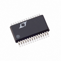
LTC2424IG Linear Technology, LTC2424IG Datasheet - Page 17

LTC2424IG
Manufacturer Part Number
LTC2424IG
Description
IC ADC 20BIT 4CH MICROPWR 28SSOP
Manufacturer
Linear Technology
Datasheet
1.LTC2424CGPBF.pdf
(36 pages)
Specifications of LTC2424IG
Number Of Bits
20
Sampling Rate (per Second)
7.5
Data Interface
MICROWIRE™, Serial, SPI™
Number Of Converters
1
Power Dissipation (max)
1mW
Voltage Supply Source
Single Supply
Operating Temperature
-40°C ~ 85°C
Mounting Type
Surface Mount
Package / Case
28-SSOP (0.200", 5.30mm Width)
Lead Free Status / RoHS Status
Contains lead / RoHS non-compliant
Available stocks
Company
Part Number
Manufacturer
Quantity
Price
Part Number:
LTC2424IG#PBF
Manufacturer:
LINEAR/凌特
Quantity:
20 000
Part Number:
LTC2424IG#TRPBF
Manufacturer:
LINEAR/凌特
Quantity:
20 000
APPLICATIONS
For output data rates up to 50 samples/second, the total
unadjusted error (TUE) is better than 16 bits, and better
than 12 bits at 100 samples/second. As shown in Figure 8,
for output data rates of 100 samples/second, the TUE is
better than 15 bits for V
unaveraged total unadjusted error for the LTC2424 or
LTC2428 operating at 100 samples/second with V
2.5V. Figure 10 shows the same device operating with a 5V
reference and an output data rate of 7.5 samples/second.
At 100 samples/second, the LTC2424/LTC2428 can be
used to capture transient data. This is useful for monitor-
ing settling or auto gain ranging in a system. The LTC2424/
LTC2428 can monitor signals at an output rate of 100
samples/second. After acquiring 100 samples/second data,
the F
110dB and the highest possible DC accuracy. The no
latency architecture of the LTC2424/LTC2428 allows con-
secutive readings (one at 100 samples/second the next at
7.5 samples/second) without interaction between the two
readings.
As shown in Figure 11, the LTC2424/LTC2428 can cap-
ture transient data with 90dB of dynamic range (with a
300mV
performance of the LTC2424/LTC2428 enables signals to
be digitized independent of a large DC offset. Figures 12a
and 12b show the dynamic performance with a 15Hz
signal superimposed on a 2V DC level. The same signal
with no DC level is shown in Figures 12c and 12d.
SERIAL INTERFACE
The LTC2424/LTC2428 transmit the conversion results,
program the channel selection, and receive the start of
conversion command through a synchronous 4-wire in-
terface (SCK = CLK, CSADC = CSMUX). During the conver-
sion and sleep states, this interface can be used to assess
the converter status. While in the sleep state this interface
may be used to program an input channel. During the data
output state, it is used to read the conversion result.
ADC Serial Clock Input/Output (SCK)
The serial clock signal present on SCK (Pin 25) is used to
synchronize the data transfer. Each bit of data is shifted out
of the SDO pin on the falling edge of the serial clock.
O
pin may be driven LOW enabling 60Hz rejection to
P-P
input signal at 2Hz). The exceptional DC
U
REF
INFORMATION
U
below 2.5V. Figure 9 shows an
W
U
REF
=
Figure 8. Total Error vs V
256
224
192
160
128
–20
–25
–30
–40
–10
–10
–15
–35
96
64
32
–2
–4
–6
–8
10
–5
0
6
4
2
0
5
0
1.0
Figure 10. Total Unadjusted Error at
7.5 Samples/Second (No Averaging)
Figure 9. Total Unadjusted Error at
100 Samples/Second (No Averaging)
0
0
OUTPUT RATE = 100sps
1.5
2.0
REFERENCE VOLTAGE (V)
INPUT VOLTAGE (V)
INPUT VOLTAGE (V)
LTC2424/LTC2428
2.5
3.0
REF
3.5
(Output Rate = 100sps)
4.0
12 BITS
13 BITS
14 BITS
15 BITS
V
V
CC
REF
V
V
CC
REF
4.5
= 5V
24248 F08
= 2.5V
24248 F10
= 5V
24248 F09
= 5V
5.0
2.5
5
17


