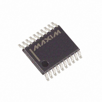
MAX1149BEUP+ Maxim Integrated Products, MAX1149BEUP+ Datasheet - Page 5

MAX1149BEUP+
Manufacturer Part Number
MAX1149BEUP+
Description
IC ADC 14BIT 116KSPS 20-TSSOP
Manufacturer
Maxim Integrated Products
Datasheet
1.MAX1147BEUP.pdf
(25 pages)
Specifications of MAX1149BEUP+
Number Of Bits
14
Sampling Rate (per Second)
116k
Data Interface
MICROWIRE™, QSPI™, Serial, SPI™
Number Of Converters
1
Power Dissipation (max)
879mW
Voltage Supply Source
Single Supply
Operating Temperature
-40°C ~ 85°C
Mounting Type
Surface Mount
Package / Case
20-TSSOP
Number Of Adc Inputs
8
Architecture
SAR
Conversion Rate
116 KSPs
Resolution
14 bit
Interface Type
Serial
Voltage Reference
Internal 2.5 V or External
Supply Voltage (max)
3.3 V
Mounting Style
SMD/SMT
Lead Free Status / RoHS Status
Lead free / RoHS Compliant
TIMING CHARACTERISTICS
(V
external clock (50% duty cycle), 18 clocks/conversion (116ksps), V
for the MAX1146/MAX1148, external 2.500V reference at REF for the MAX1147/MAX1149, T
Typical values are at T
Note 1: Tested at V
Note 2: Relative accuracy is the deviation of the analog value at any code from its theoretical value after the full-scale range has
Note 3: Offset nulled. Measured with external reference.
Note 4: “On” channel grounded; full-scale 1kHz sine wave applied to all “off” channels.
Note 5: Conversion time defined as the number of clock cycles multiplied by the clock period; clock has 50% duty cycle. (See
Note 6: The common-mode range for the analog inputs is from AGND to V
Note 7: Digital inputs equal V
Note 8: External load should not change during conversion for specified accuracy.
Note 9: Measured as (V
DIN to SCLK Setup Time
DIN to SCLK Hold Time
SCLK Fall to Output Data Valid
CS Fall to DOUT Enable
CS Rise to DOUT Disable
SHDN Rise CS Fall to SCLK Rise
Time
SHDN Rise CS Fall to SCLK Rise
Hold Time
SCLK Clock Frequency
SCLK Pulse-Width High
SCLK Pulse-Width Low
CS Fall to SSTRB Output Enable
CS Rise to SSTRB Output Disable
SSTRB Rise to SCLK Rise
SCLK Fall to SSTRB Edge
CS Pulse Width
DD
= 4.75V to 5.25V (MAX1146/MAX1148), V
been calibrated.
Figures 8–11.)
MAX1146/MAX1148. V
PARAMETER
_______________________________________________________________________________________
DD
A
= +25°C.) (Figures 1, 2, and 3)
= 3.0V (MAX1147/MAX1149) or 5.0V(MAX1146/MAX1148); V
FS
x 3.6V) - (V
DD
DD
or DGND.
= 3.6V to 2.7V for MAX1147/MAX1149 and V
SYMBOL
f
t
FS
t
t
t
t
t
t
t
SCLK
t
SCST
t
DOD
CSW
t
DOV
DOE
CSH
t
SCK
t
CSS
t
STD
STE
DH
CH
DS
CL
x 2.7V) for the MAX1147/MAX1149 and (V
Multichannel, True-Differential,
DD
C
C
C
External clock mode
Internal clock mode
Internal clock mode
Internal clock mode
External clock mode only
External clock mode only
Internal clock mode only
LOAD
LOAD
LOAD
= 2.7V to 3.6V (MAX1147/MAX1149), SHDN = V
= 50pF
= 50pF
= 50pF
CONDITIONS
REFADJ
= V
DD
.
DD
DD
Serial, 14-Bit ADCs
, C
= 5.25V to 4.75V for the MAX1146/MAX1148.
FS
REF
COM
x 5.25V) - (V
= 2.2µF, external +4.096V reference at REF
= 0; unipolar single-ended input mode.
A
= T
MIN
MIN
100
100
100
0.1
50
10
50
50
0
0
FS
DD
to T
x 4.75V) for the
, V
MAX
COM
TYP
, unless otherwise noted.
0
= 0, f
MAX
120
120
120
120
SCLK
2.1
2.1
80
80
= 2.1MHz,
UNITS
MHz
ns
ns
ns
ns
ns
ns
ns
ns
ns
ns
ns
ns
ns
ns
5


