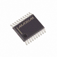
MAX1149BEUP+ Maxim Integrated Products, MAX1149BEUP+ Datasheet - Page 11

MAX1149BEUP+
Manufacturer Part Number
MAX1149BEUP+
Description
IC ADC 14BIT 116KSPS 20-TSSOP
Manufacturer
Maxim Integrated Products
Datasheet
1.MAX1147BEUP.pdf
(25 pages)
Specifications of MAX1149BEUP+
Number Of Bits
14
Sampling Rate (per Second)
116k
Data Interface
MICROWIRE™, QSPI™, Serial, SPI™
Number Of Converters
1
Power Dissipation (max)
879mW
Voltage Supply Source
Single Supply
Operating Temperature
-40°C ~ 85°C
Mounting Type
Surface Mount
Package / Case
20-TSSOP
Number Of Adc Inputs
8
Architecture
SAR
Conversion Rate
116 KSPs
Resolution
14 bit
Interface Type
Serial
Voltage Reference
Internal 2.5 V or External
Supply Voltage (max)
3.3 V
Mounting Style
SMD/SMT
Lead Free Status / RoHS Status
Lead free / RoHS Compliant
MAX1148
MAX1149
10
11
12
13
14
15
16
17
18
19
20
—
1
2
3
4
5
6
7
8
9
PIN
MAX1146
MAX1147
5–8
—
—
—
—
10
11
12
13
14
15
16
17
18
19
20
1
2
3
4
9
______________________________________________________________________________________
REFADJ
SSTRB
NAME
AGND
DGND
SHDN
DOUT
SCLK
COM
CH0
CH1
CH2
CH3
CH4
CH5
CH6
CH7
N.C.
REF
V
DIN
CS
DD
Analog Inputs
Common Input. Negative analog input in single-ended mode. COM sets zero-code voltage in
unipolar and bipolar mode.
Active-Low Shutdown Input. Pulling SHDN low shuts down the device reducing supply current
to 0.2µA. Driving shutdown high enables the devices.
Reference-Buffer Output/ADC Reference Input. Reference voltage for analog-to-digital
conversion. In internal reference mode, the MAX1146/MAX1148 V
MAX1147/MAX1149 V
Bandgap Reference Output and Reference Buffer Input. Bypass to AGND with a 0.01µF
capacitor. Connect REFADJ to V
buffer amplifier.
Analog Ground
Digital Ground
Serial Data Output. Data is clocked out at the falling edge of SCLK when CS is low. DOUT is
high impedance when CS is high.
Serial Strobe Output. In internal clock mode, SSTRB goes low when the ADC conversion
begins, and goes high when the conversion is finished. In external clock mode, SSTRB pulses
high for two clock periods before the MSB decision. SSTRB is high impedance when CS is high
(external clock mode).
Serial Data Input. Data is clocked in at the rising edge of SCLK when CS is low. DIN is high
impedance when CS is high.
Active-Low Chip Select. Data is not clocked into DIN unless CS is low. When CS is high, DOUT
is high impedance.
Serial Clock Input. Clocks data in and out of the serial interface and sets the conversion speed
in external clock mode. (Duty cycle must be 40% to 60%.)
Positive Supply Voltage. Bypass to AGND with a 0.1µF capacitor.
No Connection. Not internally connected.
Multichannel, True-Differential,
REF
is +2.500V.
DD
to disable the internal bandgap reference and reference-
FUNCTION
Serial, 14-Bit ADCs
REF
Pin Description
is +4.096V, and the
11


