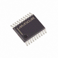
MAX1149BEUP+ Maxim Integrated Products, MAX1149BEUP+ Datasheet - Page 19

MAX1149BEUP+
Manufacturer Part Number
MAX1149BEUP+
Description
IC ADC 14BIT 116KSPS 20-TSSOP
Manufacturer
Maxim Integrated Products
Datasheet
1.MAX1147BEUP.pdf
(25 pages)
Specifications of MAX1149BEUP+
Number Of Bits
14
Sampling Rate (per Second)
116k
Data Interface
MICROWIRE™, QSPI™, Serial, SPI™
Number Of Converters
1
Power Dissipation (max)
879mW
Voltage Supply Source
Single Supply
Operating Temperature
-40°C ~ 85°C
Mounting Type
Surface Mount
Package / Case
20-TSSOP
Number Of Adc Inputs
8
Architecture
SAR
Conversion Rate
116 KSPs
Resolution
14 bit
Interface Type
Serial
Voltage Reference
Internal 2.5 V or External
Supply Voltage (max)
3.3 V
Mounting Style
SMD/SMT
Lead Free Status / RoHS Status
Lead free / RoHS Compliant
Method 1 allows the direct application of an external
reference from 1.5V to V
impedance is typically 10kΩ. During conversion, an
external reference at REF must deliver up to 210µA and
have an output impedance less than 10Ω. Bypass REF
with a 0.1µF capacitor to AGND to improve its output
impedance.
Method 2 utilizes the internal reference buffer to reduce
the external reference load. The REFADJ input imped-
ance is typically 20kΩ. During a conversion, an external
reference at REFADJ must deliver at least 100µA and
have an output impedance less than 100Ω. The
MAX1146/MAX1148 reference buffer has a 3.277V/V
gain and the MAX1147/MAX1149 has a gain of
2.000V/V. The external reference voltage at REFADJ
multiplied by the reference buffer gain is the SAR ADC
reference voltage. This reference appears at REF and
must be from 1.5V to V
Figure 12. External Reference Applied to REF
Table 7. Full Scale and Zero Scale
Note: The common mode range for the analog inputs is from AGND to V
MAX1146–
MAX1149
INPUT AND OUTPUT
Single-Ended Mode
Differential Mode
MODES
REFERENCE
BANDGAP
SAR
ADC
1.250V
REFERENCE
DISABLED
BUFFER
REF
______________________________________________________________________________________
20kΩ
DD
DGND
AGND
REF
V
DD
DD
+ 50mV. Bypass REFADJ
ZERO SCALE
REFADJ
+ 50mV. The REF input
V
V
COM
0.1µF
0.1µF
IN-
3.000V
UNIPOLAR MODE
+5V
OUT
Multichannel, True-Differential,
MAX6163
GND
+5V
IN
FULL SCALE
V
V
REF
REF
+ V
+ V
COM
IN-
with a 0.01µF capacitor and bypass REF with a 2.2µF
capacitor to AGND.
Table 7 shows the full-scale voltage ranges for unipolar
and bipolar modes.
Output data coding for the MAX1146–MAX1149 is bina-
ry in unipolar mode and two’s complement binary in
bipolar mode with 1 LSB = (V
number of bits (14). Code transitions occur halfway
between successive-integer LSB values. Figure 14 and
Figure 15 show the input/output (I/O) transfer functions
for unipolar and bipolar operations, respectively.
The MAX1146–MAX1149 feature a serial interface that
is fully compatible with SPI, QSPI, and MICROWIRE. If a
serial interface is available, establish the CPU’s serial
interface as a master, so that the CPU generates the
serial clock for the ADCs. Select a clock frequency up
to 2.1MHz.
When using an SPI (Figure 16a) or MICROWIRE interface
(Figure 16b), set CPOL = CPHA = 0. Two 8-bit readings
are necessary to obtain the entire 14-bit result from the
ADC. DOUT data transitions on the serial clock’s falling
Figure 13. Reference Adjust Circuit
DD
NEGATIVE FULL
−
.
V
−
REF
2
V
100kΩ
24kΩ
SCALE
REF
2
Serial, 14-Bit ADCs
+
+3.3V
+
V
COM
V
IN
−
510kΩ
BIPOLAR MODE
ZERO SCALE
SPI and MICROWIRE Interface
0.047µF
V
V
COM
IN-
REF
Transfer Function
Serial Interfaces
/2
REFADJ
N
MAX1146–
), where N is the
MAX1149
POSITIVE FULL
+
+
V
V
REF
2
REF
2
SCALE
+
+
V
V
COM
IN
−
19


