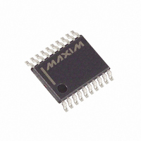
MAX1149BEUP+ Maxim Integrated Products, MAX1149BEUP+ Datasheet - Page 22

MAX1149BEUP+
Manufacturer Part Number
MAX1149BEUP+
Description
IC ADC 14BIT 116KSPS 20-TSSOP
Manufacturer
Maxim Integrated Products
Datasheet
1.MAX1147BEUP.pdf
(25 pages)
Specifications of MAX1149BEUP+
Number Of Bits
14
Sampling Rate (per Second)
116k
Data Interface
MICROWIRE™, QSPI™, Serial, SPI™
Number Of Converters
1
Power Dissipation (max)
879mW
Voltage Supply Source
Single Supply
Operating Temperature
-40°C ~ 85°C
Mounting Type
Surface Mount
Package / Case
20-TSSOP
Number Of Adc Inputs
8
Architecture
SAR
Conversion Rate
116 KSPs
Resolution
14 bit
Interface Type
Serial
Voltage Reference
Internal 2.5 V or External
Supply Voltage (max)
3.3 V
Mounting Style
SMD/SMT
Lead Free Status / RoHS Status
Lead free / RoHS Compliant
Multichannel, True-Differential,
Serial, 14-Bit ADCs
Figure 19 shows an application circuit to interface the
MAX1146–MAX1149 to the TMS320 in external clock
mode. The timing diagram for this interface circuit is
shown in Figure 20. Use the following steps to initiate a
conversion in the MAX1146–MAX1149 and to read the
results:
1) The TMS320 should be configured with CLKX
2) Drive the CS of the MAX1146–MAX1149 low
3) Write an 8-bit word (1XXXXX11) to the
4) The MAX1146–MAX1149 SSTRB output is moni-
5) The TMS320 reads in one data bit on each of the
6) Pull CS high to disable the MAX1146–MAX1149
Figure 20. TMS320 Serial-Interface Timing Diagram
22
SSTRB
DOUT
SCLK
DIN
CS
(transmit clock) as an active-high output clock and
CLKR (TMS320 receive clock) as an active-high
input clock. CLKX and CLKR on the TMS320 are
connected together with the MAX1146–MAX1149
SCLK input.
through the XF_ I/O port of the TMS320 to clock
data into the MAX1146–MAX1149 DIN.
MAX1146–MAX1149 to initiate a conversion and
place the device into external clock mode. Refer to
Table 1 to select the proper XXXXX bit values for
your specific application.
tored by the FSR input of the TMS320. A falling
edge on the SSTRB output indicates that the con-
version is in progress and data is ready to be
received from the MAX1146–MAX1149.
next 16 rising edges of SCLK. These data bits rep-
resent the 14-bit conversion result followed by 2
trailing bits, which should be ignored.
until the next conversion is initiated.
______________________________________________________________________________________
START
SEL2
SEL1
TMS32OLC3x Interface
SEL0
SGL/DIF
UNI/BIP
PD1
Careful PC board layout is essential for best system
performance. Boards should have separate analog and
digital ground planes. Ensure that digital and analog
signals are separated from each other. Do not run ana-
log and digital (especially clock) lines parallel to one
another, or digital lines underneath the device pack-
age.
Figure 4 shows the recommended system ground con-
nections. Establish an analog ground point at AGND
and a digital ground point at DGND. Connect all analog
grounds to the star analog ground. Connect the digital
grounds to the star digital ground. Connect the digital
ground point to the analog ground point directly at the
device. For lowest noise operation, the ground return to
the star ground’s power supply should be low imped-
ance and as short as possible.
Figure 19. MAX1146–MAX1149-to-TMS320 Serial Interface
PD0
TMS320LC3x
Layout, Grounding, and Bypassing
CLKX
CLKR
MSB
FSR
DX
DR
XF
B12
B1
CS
SCLK
DIN
DOUT
SSTRB
LSB
MAX1146–
MAX1149
HIGH-Z
HIGH-Z


