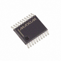
MAX1149BEUP+ Maxim Integrated Products, MAX1149BEUP+ Datasheet - Page 2

MAX1149BEUP+
Manufacturer Part Number
MAX1149BEUP+
Description
IC ADC 14BIT 116KSPS 20-TSSOP
Manufacturer
Maxim Integrated Products
Datasheet
1.MAX1147BEUP.pdf
(25 pages)
Specifications of MAX1149BEUP+
Number Of Bits
14
Sampling Rate (per Second)
116k
Data Interface
MICROWIRE™, QSPI™, Serial, SPI™
Number Of Converters
1
Power Dissipation (max)
879mW
Voltage Supply Source
Single Supply
Operating Temperature
-40°C ~ 85°C
Mounting Type
Surface Mount
Package / Case
20-TSSOP
Number Of Adc Inputs
8
Architecture
SAR
Conversion Rate
116 KSPs
Resolution
14 bit
Interface Type
Serial
Voltage Reference
Internal 2.5 V or External
Supply Voltage (max)
3.3 V
Mounting Style
SMD/SMT
Lead Free Status / RoHS Status
Lead free / RoHS Compliant
ABSOLUTE MAXIMUM RATINGS
V
AGND to DGND.....................................................-0.3V to +0.3V
CH0–CH7, COM to AGND..........................-0.3V to (V
REF, REFADJ to AGND ..............................-0.3V to (V
Digital Inputs to DGND...............................-0.3V to (V
Digital Outputs to DGND ............................-0.3V to (V
Digital Output Sink Current .................................................25mA
Multichannel, True-Differential,
Serial, 14-Bit ADCs
Stresses beyond those listed under “Absolute Maximum Ratings” may cause permanent damage to the device. These are stress ratings only, and functional
operation of the device at these or any other conditions beyond those indicated in the operational sections of the specifications is not implied. Exposure to
absolute maximum rating conditions for extended periods may affect device reliability.
ELECTRICAL CHARACTERISTICS
(V
duty cycle), 18 clocks/conversion (116ksps), V
MAX1148), external 2.500V reference at REF (MAX1147/MAX1149), T
T
2
DD
A
DC ACCURACY (Note 1)
Resolution
Relative Accuracy (Note 2)
Differential Nonlinearity
Offset Error
Offset Temperature Coefficient
Gain Error
Gain Temperature Coefficient
Channel-to-Channel Offset
Matching
Channel-to-Channel Gain
Matching
DYNAMIC SPECIFICATIONS (1kHz sine-wave input, 2.5V P-P , full-scale analog input, 116ksps, 2.1MHz external clock)
Signal-to-Noise Plus Distortion
Ratio
Total Harmonic Distortion
Spurious-Free Dynamic Range
Channel-to-Channel Crosstalk
Small-Signal Bandwidth
Full-Power Bandwidth
CONVERSION RATE
Conversion Time (Note 5)
DD
= +25°C.)
_______________________________________________________________________________________
to AGND, DGND ............................................-0.3V to +6.0V
= 5V (MAX1146/MAX1148), V
PARAMETER
DD
SYMBOL
t CONV
SINAD
= 3.3V (MAX1147/MAX1149),
SSBW
FPBW
SFDR
DNL
THD
INL
No missing codes over temperature
(Note 3)
Up to the 5th harmonic
(Note 4)
-3dB point
SINAD > 68dB
External clock, 2.1MHz 15 SCLK cycles
Internal clock
REFADJ
DD
DD
DD
DD
+ 0.3V)
+ 0.3V)
+ 0.3V)
+ 0.3V)
= V
DD
CONDITIONS
, C
REF
Continuous Power Dissipation (T
Operating Temperature Ranges
Storage Temperature Range .............................-60°C to +150°C
Lead Temperature (soldering, 10s) .................................+300°C
SHDN = V
A
= T
20 TSSOP (derate 10.9mW/°C above +70°C) .............879mW
MAX114_ BC_ _ ..................................................0°C to +70°C
MAX114_ BE_ _ ...............................................-40°C to +85°C
= 2.2µF, external +4.096V reference at REF (MAX1146/
MIN
to T
DD
, V
MAX
COM
, unless otherwise noted. Typical values are at
= 0, f
SCLK
MIN
-1.0
7.2
14
77
84
6
A
= 2.1MHz, external clock (50%
= +70°C)
±0.7
±0.5
±0.8
TYP
0.3
-96
-85
3.0
2.0
±1
±1
81
98
MAX
+1.5
±10
±20
-88
±2
8
ppm/°C
ppm/°C
UNITS
MHz
MHz
LSB
LSB
LSB
LSB
LSB
LSB
Bits
dB
dB
dB
dB
µs


